What is Global Semiconductor Sputtering Targets Market?
The Global Semiconductor Sputtering Targets Market is a crucial component of the semiconductor industry, which is the backbone of modern electronics. Sputtering targets are materials used in the sputtering process, a method to deposit thin films on substrates, which is essential in the manufacturing of semiconductors. These targets are made from various materials, including metals, alloys, and non-metals, and are used to create the thin layers that form the intricate circuits in semiconductor devices. The market for these sputtering targets is driven by the increasing demand for semiconductors in various applications, such as consumer electronics, automotive, and telecommunications. As technology advances, the need for more efficient and smaller semiconductor devices grows, further propelling the demand for high-quality sputtering targets. The market is characterized by continuous innovation and development to meet the evolving needs of the semiconductor industry, ensuring that manufacturers can produce the next generation of electronic devices. The global market for semiconductor sputtering targets is expected to grow significantly, driven by technological advancements and the increasing adoption of semiconductors in various industries.
Metal Sputtering Target Material, Alloy Sputtering Target Material, Non-metal Sputtering Target Material in the Global Semiconductor Sputtering Targets Market:
Metal sputtering target materials are a significant segment of the Global Semiconductor Sputtering Targets Market. These materials are primarily composed of pure metals such as aluminum, copper, titanium, and tantalum. Metal sputtering targets are widely used due to their excellent electrical conductivity and ability to form uniform thin films, which are essential for creating the conductive pathways in semiconductor devices. Aluminum, for example, is commonly used in the interconnect layers of integrated circuits due to its low resistivity and cost-effectiveness. Copper has gained popularity as a sputtering target material because of its superior conductivity and electromigration resistance, making it ideal for advanced semiconductor applications. Titanium and tantalum are often used as barrier layers to prevent the diffusion of other materials, ensuring the integrity and performance of the semiconductor device. Alloy sputtering target materials, on the other hand, are composed of two or more metallic elements combined to achieve specific properties that are not attainable with pure metals. These materials are engineered to enhance certain characteristics such as hardness, corrosion resistance, and thermal stability. Common alloy sputtering targets include aluminum-copper, titanium-tungsten, and nickel-chromium. The use of alloy sputtering targets allows for the customization of thin film properties to meet the specific requirements of different semiconductor applications. For instance, aluminum-copper alloys are used to improve the electromigration resistance of interconnects, while titanium-tungsten alloys are employed in contact layers to enhance adhesion and reduce contact resistance. Non-metal sputtering target materials are another important category in the semiconductor sputtering targets market. These materials include ceramics, compounds, and other non-metallic substances such as silicon dioxide, silicon nitride, and aluminum oxide. Non-metal sputtering targets are used to deposit insulating or dielectric layers in semiconductor devices, which are crucial for isolating different components and preventing electrical interference. Silicon dioxide, for example, is widely used as a dielectric material in metal-oxide-semiconductor (MOS) devices due to its excellent insulating properties and compatibility with silicon. Silicon nitride is another popular non-metal sputtering target material, known for its high thermal stability and mechanical strength, making it suitable for protective coatings and passivation layers. Aluminum oxide is often used in applications requiring high hardness and wear resistance, such as protective coatings for optical devices. The choice of sputtering target material depends on the specific requirements of the semiconductor device being manufactured. Factors such as electrical conductivity, thermal stability, mechanical strength, and chemical compatibility are considered when selecting the appropriate material. The development of new materials and the optimization of existing ones are ongoing processes in the semiconductor sputtering targets market, driven by the need to improve device performance and meet the demands of emerging technologies. As the semiconductor industry continues to evolve, the demand for advanced sputtering target materials is expected to grow, supporting the production of smaller, faster, and more efficient electronic devices.
Wafer Manufacturing, Packaging and Testing in the Global Semiconductor Sputtering Targets Market:
The Global Semiconductor Sputtering Targets Market plays a vital role in various stages of semiconductor manufacturing, including wafer manufacturing, packaging, and testing. In wafer manufacturing, sputtering targets are used to deposit thin films on silicon wafers, which are the foundational substrates for semiconductor devices. The sputtering process involves bombarding the target material with high-energy particles, causing atoms to be ejected and deposited onto the wafer surface. This technique is used to create the multiple layers of conductive, insulating, and semiconducting materials that form the intricate circuits in semiconductor devices. The precision and uniformity of the thin films deposited using sputtering targets are crucial for the performance and reliability of the final semiconductor product. In the packaging stage, sputtering targets are used to deposit protective and functional coatings on semiconductor chips. These coatings serve various purposes, such as enhancing thermal conductivity, providing electrical insulation, and protecting the chip from environmental factors. For example, metal sputtering targets like aluminum and copper are used to create interconnects and bonding pads, which facilitate the electrical connection between the chip and the external circuitry. Non-metal sputtering targets, such as silicon dioxide and silicon nitride, are used to deposit dielectric layers that provide electrical insulation and protect the chip from moisture and contaminants. The choice of sputtering target material and the deposition process are critical factors in ensuring the reliability and performance of the packaged semiconductor device. In the testing phase, sputtering targets are used to create test structures and calibration standards on semiconductor wafers. These structures are essential for evaluating the electrical and mechanical properties of the semiconductor device, ensuring that it meets the required specifications and performance standards. Sputtering targets are used to deposit thin films with precise thickness and composition, enabling accurate testing and characterization of the semiconductor device. The use of sputtering targets in the testing phase helps manufacturers identify defects and optimize the manufacturing process, ensuring the production of high-quality semiconductor devices. The Global Semiconductor Sputtering Targets Market is driven by the increasing demand for advanced semiconductor devices in various applications, such as consumer electronics, automotive, telecommunications, and industrial automation. As technology continues to advance, the need for smaller, faster, and more efficient semiconductor devices grows, driving the demand for high-quality sputtering targets. The market is characterized by continuous innovation and development, with manufacturers investing in research and development to create new materials and improve existing ones. The development of advanced sputtering target materials and deposition techniques is essential for meeting the evolving needs of the semiconductor industry and supporting the production of the next generation of electronic devices.
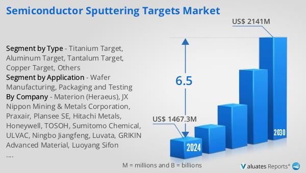
Global Semiconductor Sputtering Targets Market Outlook:
In 2024, the global market for semiconductor sputtering targets was valued at approximately $2,193 million. This market is anticipated to experience significant growth over the coming years, with projections indicating that it will reach an estimated size of $3,458 million by 2031. This growth trajectory represents a compound annual growth rate (CAGR) of 6.8% throughout the forecast period. The increasing demand for semiconductors across various industries, including consumer electronics, automotive, and telecommunications, is a key driver of this market expansion. As technology continues to advance, the need for more efficient and smaller semiconductor devices becomes more pronounced, further fueling the demand for high-quality sputtering targets. The market's growth is also supported by continuous innovation and development in sputtering target materials and deposition techniques, which are essential for meeting the evolving needs of the semiconductor industry. Manufacturers are investing in research and development to create new materials and improve existing ones, ensuring that they can produce the next generation of electronic devices. The global semiconductor sputtering targets market is poised for significant growth, driven by technological advancements and the increasing adoption of semiconductors in various applications.
| Report Metric | Details |
| Report Name | Semiconductor Sputtering Targets Market |
| Accounted market size in year | US$ 2193 million |
| Forecasted market size in 2031 | US$ 3458 million |
| CAGR | 6.8% |
| Base Year | year |
| Forecasted years | 2025 - 2031 |
| by Type |
|
| by Application |
|
| Production by Region |
|
| Consumption by Region |
|
| By Company | JX Advanced Metals, Materion, Konfoong Materials International, Linde, Proterial, Plansee SE, TOSOH, Honeywell, Grinm Advanced Materials Co., Ltd., ULVAC, TANAKA, Sumitomo Chemical, Luvata, Advantec, Longhua Technology Group (Luoyang), Furuya Metal, Umicore Thin Film Products, Angstrom Sciences |
| Forecast units | USD million in value |
| Report coverage | Revenue and volume forecast, company share, competitive landscape, growth factors and trends |


