What is Global 4D Scanning Transmission Electron Microscopy (4D STEM) Market?
Global 4D Scanning Transmission Electron Microscopy (4D STEM) is a cutting-edge technology that has revolutionized the field of electron microscopy by providing a four-dimensional view of materials at the atomic level. Unlike traditional electron microscopy, which typically offers two-dimensional images, 4D STEM captures data in four dimensions, including two spatial dimensions, time, and energy or momentum. This allows researchers to gain a more comprehensive understanding of the material's structure, properties, and behavior. The technology is particularly valuable in fields such as materials science, nanotechnology, and life sciences, where understanding the intricate details of materials at the atomic scale is crucial. By using a focused electron beam that scans across the sample, 4D STEM collects a vast amount of data that can be analyzed to reveal information about the sample's composition, crystallography, and electronic properties. This advanced microscopy technique is instrumental in driving innovations and discoveries, as it enables scientists to visualize and analyze materials in ways that were previously impossible. As a result, the global market for 4D STEM is experiencing significant growth, driven by the increasing demand for high-resolution imaging and analysis in various scientific and industrial applications.
Monolithic Active Pixel Sensor (MAPS), Hybrid Pixel Array Detector (PAD) in the Global 4D Scanning Transmission Electron Microscopy (4D STEM) Market:
Monolithic Active Pixel Sensor (MAPS) and Hybrid Pixel Array Detector (PAD) are two critical components in the realm of Global 4D Scanning Transmission Electron Microscopy (4D STEM) that have significantly enhanced the capabilities of this advanced imaging technology. MAPS are integrated circuits that contain an array of pixel sensors, each capable of detecting and processing incoming electrons. These sensors are monolithic, meaning they are fabricated on a single silicon wafer, which allows for a compact design and high spatial resolution. The integration of MAPS in 4D STEM systems has improved the sensitivity and speed of data acquisition, enabling researchers to capture high-quality images and data with greater efficiency. The compact nature of MAPS also allows for the development of smaller and more portable electron microscopes, making the technology more accessible to a wider range of users. On the other hand, Hybrid Pixel Array Detectors (PAD) are another type of detector used in 4D STEM that combines the advantages of both direct and indirect detection methods. Hybrid PADs consist of a pixelated sensor layer bonded to a readout chip, which processes the signals generated by the incoming electrons. This hybrid approach allows for high sensitivity and dynamic range, making it possible to capture detailed images of samples with varying levels of contrast. The use of PADs in 4D STEM systems has enhanced the ability to study complex materials and biological specimens, as they can provide high-resolution images with minimal noise and distortion. Additionally, the fast readout capabilities of PADs enable real-time imaging and analysis, which is crucial for studying dynamic processes and reactions at the atomic level. The integration of MAPS and PADs in 4D STEM systems has opened up new possibilities for research and development across various scientific disciplines. In materials science, these advanced detectors allow researchers to study the atomic structure and composition of materials with unprecedented detail, leading to the discovery of new materials and the optimization of existing ones. In life sciences, the ability to visualize biological specimens at the molecular level has provided insights into cellular processes and disease mechanisms, paving the way for the development of new diagnostic and therapeutic strategies. Furthermore, the enhanced imaging capabilities of 4D STEM have applications in fields such as nanotechnology, semiconductor research, and environmental science, where understanding the properties and behavior of materials at the nanoscale is essential. Overall, the advancements in detector technology, exemplified by MAPS and PADs, have played a crucial role in the evolution of 4D STEM, making it a powerful tool for scientific exploration and innovation. As the demand for high-resolution imaging and analysis continues to grow, the development and integration of these advanced detectors will remain a key focus in the ongoing advancement of 4D STEM technology.
Materials Science, Life Sciences, Others in the Global 4D Scanning Transmission Electron Microscopy (4D STEM) Market:
The Global 4D Scanning Transmission Electron Microscopy (4D STEM) Market has found extensive applications in various fields, including materials science, life sciences, and other areas, due to its ability to provide detailed insights into the atomic structure and properties of materials. In materials science, 4D STEM is used to study the composition, crystallography, and electronic properties of materials at the atomic level. This information is crucial for the development of new materials with enhanced properties, such as increased strength, conductivity, or resistance to corrosion. Researchers can use 4D STEM to analyze the effects of different processing techniques on material properties, leading to the optimization of manufacturing processes and the development of advanced materials for various applications, including aerospace, automotive, and electronics. In the field of life sciences, 4D STEM has become an invaluable tool for studying biological specimens at the molecular level. The high-resolution imaging capabilities of 4D STEM allow researchers to visualize the intricate details of cellular structures and processes, providing insights into the mechanisms of diseases and the effects of drugs at the molecular level. This information is essential for the development of new diagnostic and therapeutic strategies, as it enables scientists to understand the underlying causes of diseases and identify potential targets for treatment. Additionally, 4D STEM can be used to study the interactions between biological molecules and materials, which is important for the development of biocompatible materials and medical devices. Beyond materials science and life sciences, 4D STEM has applications in other fields, such as nanotechnology, semiconductor research, and environmental science. In nanotechnology, 4D STEM is used to study the properties and behavior of nanomaterials, which are essential for the development of new technologies and devices. The ability to visualize and analyze materials at the nanoscale is crucial for understanding their unique properties and optimizing their performance in various applications. In semiconductor research, 4D STEM is used to study the atomic structure and composition of semiconductor materials, which is essential for the development of advanced electronic devices with improved performance and efficiency. In environmental science, 4D STEM can be used to study the effects of pollutants on materials and biological specimens, providing insights into the mechanisms of environmental degradation and the development of strategies for pollution control and remediation. Overall, the Global 4D Scanning Transmission Electron Microscopy (4D STEM) Market has become an essential tool for scientific research and innovation across various fields. Its ability to provide detailed insights into the atomic structure and properties of materials has opened up new possibilities for the development of advanced materials, technologies, and strategies for addressing some of the most pressing challenges facing society today. As the demand for high-resolution imaging and analysis continues to grow, the applications of 4D STEM are expected to expand, driving further advancements in science and technology.
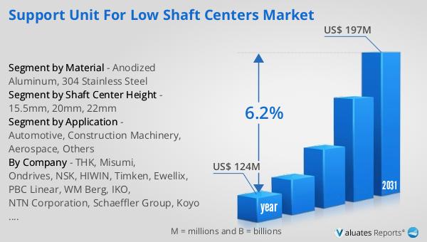
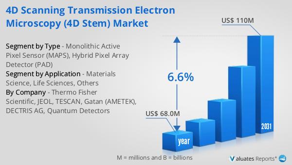
Global 4D Scanning Transmission Electron Microscopy (4D STEM) Market Outlook:
In 2024, the global market for 4D Scanning Transmission Electron Microscopy (4D STEM) was valued at approximately $68 million. This market is anticipated to grow significantly over the coming years, reaching an estimated value of $110 million by 2031. This growth trajectory represents a compound annual growth rate (CAGR) of 6.6% throughout the forecast period. The increasing demand for high-resolution imaging and analysis across various scientific and industrial applications is a key driver of this market expansion. As industries such as materials science, life sciences, and nanotechnology continue to evolve, the need for advanced microscopy techniques like 4D STEM becomes more pronounced. This technology's ability to provide detailed insights into the atomic structure and properties of materials makes it an invaluable tool for researchers and scientists. The projected growth of the 4D STEM market reflects the ongoing advancements in detector technology and the increasing adoption of this technology in research and development activities worldwide. As the market continues to expand, it is expected to play a crucial role in driving innovations and discoveries across various scientific disciplines, ultimately contributing to the advancement of science and technology on a global scale.
| Report Metric | Details |
| Report Name | 4D Scanning Transmission Electron Microscopy (4D STEM) Market |
| Accounted market size in year | US$ 68.0 million |
| Forecasted market size in 2031 | US$ 110 million |
| CAGR | 6.6% |
| Base Year | year |
| Forecasted years | 2025 - 2031 |
| Segment by Type |
|
| Segment by Application |
|
| By Region |
|
| By Company | Thermo Fisher Scientific, JEOL, TESCAN, Gatan (AMETEK), DECTRIS AG, Quantum Detectors |
| Forecast units | USD million in value |
| Report coverage | Revenue and volume forecast, company share, competitive landscape, growth factors and trends |