What is Semiconductor Single Wafer Cleaning Equipment - Global Market?
Semiconductor single wafer cleaning equipment is a crucial component in the semiconductor manufacturing process. This equipment is designed to clean individual wafers, which are thin slices of semiconductor material, typically silicon, used in the fabrication of integrated circuits and other microdevices. The cleaning process is essential to remove contaminants such as particles, organic residues, and metal ions that can affect the performance and yield of semiconductor devices. The global market for this equipment is driven by the increasing demand for semiconductors in various applications, including consumer electronics, automotive, and telecommunications. As technology advances, the need for more precise and efficient cleaning methods becomes critical, leading to innovations in cleaning equipment. The market is characterized by the presence of several key players who are continuously investing in research and development to enhance the performance and efficiency of their products. The growth of the semiconductor industry, coupled with the increasing complexity of semiconductor devices, is expected to drive the demand for single wafer cleaning equipment in the coming years. This market is also influenced by trends such as the miniaturization of electronic devices and the shift towards more environmentally friendly cleaning processes.
Wafer Size 150mm-200mm, Wafer Size 300mm, Others in the Semiconductor Single Wafer Cleaning Equipment - Global Market:
In the semiconductor single wafer cleaning equipment market, wafer sizes play a significant role in determining the type of equipment used and its efficiency. Wafer sizes typically range from 150mm to 300mm, with each size catering to different segments of the semiconductor industry. The 150mm to 200mm wafer size category is often used in the production of older semiconductor technologies and in industries where high-volume production is not as critical. These wafers are commonly found in applications such as power devices, analog devices, and some MEMS (Micro-Electro-Mechanical Systems) technologies. The equipment used for cleaning these wafers is generally less advanced compared to those used for larger wafers, but they still require precision to ensure the removal of contaminants without damaging the wafer surface. On the other hand, the 300mm wafer size is the standard for most modern semiconductor manufacturing processes. These larger wafers allow for more chips to be produced per wafer, significantly increasing production efficiency and reducing costs. The cleaning equipment for 300mm wafers is highly sophisticated, incorporating advanced technologies such as megasonic cleaning, chemical mechanical polishing, and advanced drying techniques to ensure the highest level of cleanliness and yield. The demand for 300mm wafer cleaning equipment is driven by the production of advanced semiconductor devices used in high-performance computing, data centers, and cutting-edge consumer electronics. Additionally, there are other wafer sizes, such as 450mm, which are being explored for future semiconductor manufacturing. However, the transition to these larger wafers presents significant technical and economic challenges, and the market for cleaning equipment for these sizes is still in its nascent stages. Overall, the choice of wafer size and the corresponding cleaning equipment is influenced by factors such as production volume, cost considerations, and the specific requirements of the semiconductor devices being manufactured.
IC, Semiconductor Lighting, Advanced Packaging, MEMS, Others in the Semiconductor Single Wafer Cleaning Equipment - Global Market:
Semiconductor single wafer cleaning equipment is utilized across various applications, each with its unique requirements and challenges. In the integrated circuits (IC) sector, this equipment is essential for ensuring the cleanliness and functionality of the wafers used to produce microprocessors, memory chips, and other critical components. The cleaning process in IC manufacturing is highly precise, as even the smallest contaminants can lead to defects and reduced yields. Advanced cleaning techniques, such as cryogenic aerosol cleaning and plasma cleaning, are often employed to achieve the necessary level of cleanliness. In semiconductor lighting, such as LEDs, wafer cleaning equipment plays a crucial role in removing impurities that can affect the light output and efficiency of the devices. The cleaning process must be carefully controlled to prevent damage to the delicate structures on the wafer surface. Advanced packaging, which involves the integration of multiple semiconductor devices into a single package, also relies heavily on wafer cleaning equipment. The cleaning process is critical for ensuring strong adhesion between layers and preventing contamination that could lead to device failure. In MEMS (Micro-Electro-Mechanical Systems) manufacturing, wafer cleaning equipment is used to remove particles and residues that can interfere with the mechanical and electrical functions of the devices. The cleaning process must be precise to avoid damaging the intricate structures of MEMS devices. Other applications of semiconductor single wafer cleaning equipment include the production of sensors, power devices, and RF components, where cleanliness is essential for optimal performance. Overall, the usage of this equipment is driven by the need for high-quality, reliable semiconductor devices across a wide range of industries.
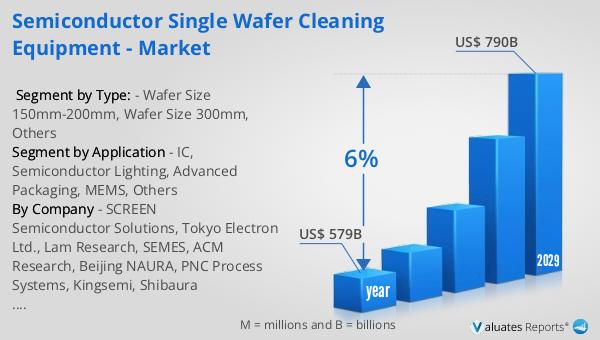
Semiconductor Single Wafer Cleaning Equipment - Global Market Outlook:
The global semiconductor market was valued at approximately $579 billion in 2022, and it is anticipated to reach around $790 billion by 2029. This growth represents a compound annual growth rate (CAGR) of 6% over the forecast period. The expansion of the semiconductor market is fueled by the increasing demand for electronic devices, advancements in technology, and the growing adoption of semiconductors in various industries such as automotive, telecommunications, and consumer electronics. As the demand for more powerful and efficient electronic devices continues to rise, the semiconductor industry is expected to experience significant growth. This growth is also supported by the ongoing development of new semiconductor technologies and the increasing complexity of semiconductor devices. The market outlook for semiconductor single wafer cleaning equipment is closely tied to the overall growth of the semiconductor industry, as the need for advanced cleaning solutions becomes more critical with the increasing complexity of semiconductor manufacturing processes. As the semiconductor market continues to expand, the demand for single wafer cleaning equipment is expected to grow, driven by the need for higher yields, improved device performance, and more efficient manufacturing processes.
| Report Metric | Details |
| Report Name | Semiconductor Single Wafer Cleaning Equipment - Market |
| Accounted market size in year | US$ 579 billion |
| Forecasted market size in 2029 | US$ 790 billion |
| CAGR | 6% |
| Base Year | year |
| Forecasted years | 2024 - 2029 |
| Segment by Type: |
|
| Segment by Application |
|
| By Region |
|
| By Company | SCREEN Semiconductor Solutions, Tokyo Electron Ltd., Lam Research, SEMES, ACM Research, Beijing NAURA, PNC Process Systems, Kingsemi, Shibaura Mechatronics |
| Forecast units | USD million in value |
| Report coverage | Revenue and volume forecast, company share, competitive landscape, growth factors and trends |


