What is Semiconductor Metrology Instrument - Global Market?
Semiconductor metrology instruments are specialized tools used to measure and analyze the physical and electrical properties of semiconductor devices and materials. These instruments are crucial in the semiconductor manufacturing process, ensuring that the components meet the required specifications and quality standards. The global market for semiconductor metrology instruments is driven by the increasing demand for semiconductors in various applications, such as consumer electronics, automotive, and telecommunications. As technology advances, the need for more precise and accurate measurement tools becomes essential, leading to the development of advanced metrology instruments. These instruments help manufacturers improve yield, reduce defects, and enhance the overall performance of semiconductor devices. The market is characterized by continuous innovation, with companies investing in research and development to create more efficient and reliable metrology solutions. The growth of the semiconductor industry, coupled with the increasing complexity of semiconductor devices, is expected to drive the demand for metrology instruments in the coming years.
Autoloading, Manual Loading in the Semiconductor Metrology Instrument - Global Market:
Autoloading and manual loading are two distinct methods used in the operation of semiconductor metrology instruments, each with its own set of advantages and challenges. Autoloading systems are designed to automate the process of loading and unloading wafers or other semiconductor materials into the metrology instrument. This automation is achieved through the use of robotic arms or other mechanical systems that can handle the delicate and precise task of moving semiconductor materials without human intervention. The primary advantage of autoloading systems is their ability to increase throughput and efficiency in the semiconductor manufacturing process. By reducing the need for manual handling, these systems minimize the risk of human error and contamination, leading to more consistent and reliable measurement results. Additionally, autoloading systems can operate continuously, allowing for 24/7 production and reducing downtime. However, the implementation of autoloading systems can be costly, requiring significant investment in equipment and infrastructure. Furthermore, these systems may require regular maintenance and calibration to ensure optimal performance, adding to the overall operational costs. On the other hand, manual loading involves the direct handling of semiconductor materials by operators, who manually place the wafers or other components into the metrology instrument. This method is often used in smaller-scale operations or in situations where the cost of implementing an autoloading system is prohibitive. Manual loading offers greater flexibility, allowing operators to quickly adapt to changes in the production process or to handle unique or specialized materials that may not be compatible with automated systems. However, manual loading is more labor-intensive and can be prone to human error, which may result in inconsistencies in measurement results. The choice between autoloading and manual loading depends on various factors, including the scale of production, budget constraints, and the specific requirements of the semiconductor manufacturing process. In many cases, a combination of both methods may be employed, with autoloading systems handling the bulk of the production while manual loading is used for specialized tasks or in situations where automation is not feasible. As the semiconductor industry continues to evolve, the demand for more efficient and reliable metrology solutions will drive the development of new technologies and methods for loading semiconductor materials into metrology instruments.
Material, Metallurgy, Biology, Medicine, Semiconductor, Others in the Semiconductor Metrology Instrument - Global Market:
Semiconductor metrology instruments play a vital role in various fields, including material science, metallurgy, biology, medicine, and, of course, the semiconductor industry itself. In material science, these instruments are used to analyze the properties of materials at the microscopic level, providing valuable insights into their structure, composition, and behavior. This information is crucial for the development of new materials with enhanced properties, such as increased strength, conductivity, or thermal resistance. In metallurgy, semiconductor metrology instruments are used to study the properties of metals and alloys, helping researchers and engineers understand how different processing techniques affect the material's performance. This knowledge is essential for the development of new metal alloys with improved characteristics, such as higher strength-to-weight ratios or better corrosion resistance. In biology and medicine, semiconductor metrology instruments are used to analyze biological samples at the molecular level, providing insights into the structure and function of biomolecules. This information is crucial for the development of new diagnostic tools and therapies, as well as for understanding the underlying mechanisms of diseases. In the semiconductor industry, metrology instruments are used to measure and analyze the properties of semiconductor devices and materials, ensuring that they meet the required specifications and quality standards. This is essential for the production of high-performance semiconductor devices, such as microprocessors, memory chips, and sensors. In addition to these fields, semiconductor metrology instruments are also used in other areas, such as environmental science, where they are used to analyze the composition of air, water, and soil samples. This information is crucial for monitoring pollution levels and assessing the impact of human activities on the environment. Overall, semiconductor metrology instruments are versatile tools that provide valuable insights into the properties and behavior of materials and devices across a wide range of fields.
Semiconductor Metrology Instrument - Global Market Outlook:
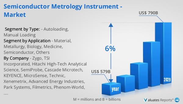
The global semiconductor market was valued at approximately $579 billion in 2022 and is anticipated to reach around $790 billion by 2029, reflecting a compound annual growth rate (CAGR) of 6% over the forecast period. This growth is driven by the increasing demand for semiconductors in various applications, such as consumer electronics, automotive, telecommunications, and industrial sectors. The rapid advancement of technology and the growing trend of digitalization are key factors contributing to the expansion of the semiconductor market. As more devices become interconnected and reliant on semiconductor components, the demand for these essential building blocks continues to rise. Additionally, the development of new technologies, such as artificial intelligence, the Internet of Things (IoT), and 5G networks, is further fueling the demand for semiconductors. These technologies require advanced semiconductor devices with higher performance, greater efficiency, and increased functionality, driving the need for continuous innovation and development in the semiconductor industry. The growth of the semiconductor market is also supported by the increasing investment in research and development, as companies strive to create more efficient and reliable semiconductor solutions. As the market continues to evolve, the demand for semiconductor metrology instruments is expected to grow, as these tools are essential for ensuring the quality and performance of semiconductor devices.
| Report Metric | Details |
| Report Name | Semiconductor Metrology Instrument - Market |
| Accounted market size in year | US$ 579 billion |
| Forecasted market size in 2029 | US$ 790 billion |
| CAGR | 6% |
| Base Year | year |
| Forecasted years | 2024 - 2029 |
| Segment by Type: |
|
| Segment by Application |
|
| By Region |
|
| By Company | Zygo, TSI Incorporated, Hitachi High-Tech Analytical Science, SemiProbe, Cascade Microtech, KEYENCE, MicroSense, Technic, Xenemetrix, Advanced Energy Industries, Park Systems, Filmetrics, Phenom-World, Hiden Analytical, Rigaku, WDI Wise Device, StellarNet, Nikon Metrology, MTI Instruments, Nanotronics Imaging, Copper Mountain Technologies, Bruker, Beijing Saifan, Shanghai Yizhi, Shanghai Aiyao |
| Forecast units | USD million in value |
| Report coverage | Revenue and volume forecast, company share, competitive landscape, growth factors and trends |


