What is Photovoltaic Monocrystalline Silicon Wafer - Global Market?
Photovoltaic monocrystalline silicon wafers are a crucial component in the solar energy industry, serving as the foundational material for solar cells. These wafers are made from a single, continuous crystal structure, which allows for higher efficiency in converting sunlight into electricity compared to their polycrystalline counterparts. The global market for these wafers is driven by the increasing demand for renewable energy sources, as countries worldwide strive to reduce their carbon footprints and transition to cleaner energy solutions. The monocrystalline silicon wafers are known for their superior performance, longevity, and efficiency, making them a preferred choice for solar panel manufacturers. As technology advances, the production processes for these wafers have become more cost-effective, further fueling their adoption in the market. The global market is characterized by significant investments in research and development, aiming to enhance the efficiency and reduce the costs of these wafers, thereby making solar energy more accessible and affordable. The market is also influenced by government policies and incentives that promote the use of renewable energy, as well as the growing awareness among consumers about the environmental benefits of solar power.
156 mm, 158 mm, 166 mm, 210 mm in the Photovoltaic Monocrystalline Silicon Wafer - Global Market:
In the global market for photovoltaic monocrystalline silicon wafers, the dimensions of the wafers play a significant role in determining their application and efficiency. The sizes 156 mm, 158 mm, 166 mm, and 210 mm refer to the diameter of the wafers, which directly impacts the surface area available for capturing sunlight. The 156 mm wafer, once a standard in the industry, is gradually being phased out in favor of larger sizes that offer better efficiency and power output. The 158 mm wafer, slightly larger, provides a marginal increase in efficiency and is often used in applications where space is limited but performance is crucial. The 166 mm wafer represents a more modern standard, offering a balance between size and efficiency, making it a popular choice for residential and commercial solar installations. Its larger surface area allows for more sunlight absorption, translating to higher energy output. The 210 mm wafer is the largest among the commonly used sizes and is primarily utilized in utility-scale solar projects where maximizing energy production is the primary goal. This size offers the highest efficiency and power output, making it ideal for large-scale solar farms. The shift towards larger wafer sizes is driven by the need to reduce the cost per watt of solar energy, as larger wafers can produce more power with fewer cells, thus lowering the overall production costs. This trend is supported by advancements in manufacturing technologies that allow for the production of larger wafers without compromising their structural integrity or performance. The global market for these wafers is highly competitive, with manufacturers constantly innovating to improve the efficiency and reduce the costs of their products. As the demand for solar energy continues to grow, the market for photovoltaic monocrystalline silicon wafers is expected to expand, with larger wafer sizes playing a crucial role in meeting the increasing energy needs. The choice of wafer size depends on various factors, including the specific application, available space, and budget constraints. Manufacturers and consumers alike must weigh these factors carefully to select the most suitable wafer size for their needs. The ongoing research and development efforts in the industry are focused on enhancing the efficiency of these wafers, exploring new materials and technologies that can further improve their performance and reduce costs. As a result, the market is poised for significant growth, driven by the increasing adoption of solar energy and the continuous advancements in wafer technology.
P-Type Battery, N-Type Battery in the Photovoltaic Monocrystalline Silicon Wafer - Global Market:
Photovoltaic monocrystalline silicon wafers are used in various types of solar cells, including P-type and N-type batteries, each with its unique characteristics and applications. P-type batteries, or P-type solar cells, are the most common type of solar cells in the market. They are made by doping silicon wafers with boron, which creates a positive charge carrier. These cells are known for their reliability and cost-effectiveness, making them a popular choice for residential and commercial solar installations. P-type cells are typically used in applications where cost is a significant consideration, and they offer a good balance between performance and affordability. However, they are more susceptible to light-induced degradation, which can affect their long-term performance. On the other hand, N-type batteries, or N-type solar cells, are made by doping silicon wafers with phosphorus, creating a negative charge carrier. These cells are known for their higher efficiency and better performance in low-light conditions compared to P-type cells. N-type cells are less prone to light-induced degradation, making them a more durable option for solar installations. They are often used in high-performance applications where efficiency is a critical factor, such as in utility-scale solar farms or in regions with less sunlight. The choice between P-type and N-type batteries depends on various factors, including the specific application, budget constraints, and performance requirements. While P-type cells offer a cost-effective solution for many applications, N-type cells provide superior performance and longevity, making them a preferred choice for high-end solar projects. The global market for photovoltaic monocrystalline silicon wafers is influenced by the demand for both P-type and N-type batteries, with manufacturers continuously innovating to improve the efficiency and reduce the costs of their products. As the solar energy industry continues to grow, the market for these wafers is expected to expand, driven by the increasing adoption of both P-type and N-type solar cells. The ongoing research and development efforts in the industry are focused on enhancing the performance of these cells, exploring new materials and technologies that can further improve their efficiency and reduce costs. As a result, the market is poised for significant growth, with both P-type and N-type batteries playing a crucial role in meeting the increasing energy needs.
Photovoltaic Monocrystalline Silicon Wafer - Global Market Outlook:
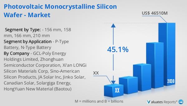
The global market for photovoltaic monocrystalline silicon wafers was valued at approximately $3,437 million in 2023. It is projected to grow significantly, reaching an estimated size of $46,510 million by 2030, with a compound annual growth rate (CAGR) of 45.1% during the forecast period from 2024 to 2030. This remarkable growth is driven by the increasing demand for renewable energy solutions and the continuous advancements in solar technology. According to the International Energy Agency, China holds a dominant position in the global market, with its market share in all key products of the supply chain exceeding 80%. This dominance is attributed to China's robust manufacturing capabilities, government support, and strategic investments in the solar energy sector. The country's focus on renewable energy and its commitment to reducing carbon emissions have positioned it as a leader in the photovoltaic monocrystalline silicon wafer market. As the demand for solar energy continues to rise, the global market is expected to witness substantial growth, with China playing a pivotal role in shaping the industry's future. The market's expansion is also supported by favorable government policies, technological advancements, and the growing awareness of the environmental benefits of solar power. As a result, the photovoltaic monocrystalline silicon wafer market is poised for significant growth, driven by the increasing adoption of solar energy and the continuous advancements in wafer technology.
| Report Metric | Details |
| Report Name | Photovoltaic Monocrystalline Silicon Wafer - Market |
| Forecasted market size in 2030 | US$ 46510 million |
| CAGR | 45.1% |
| Forecasted years | 2024 - 2030 |
| Segment by Type: |
|
| Segment by Application |
|
| By Region |
|
| By Company | GCL-Poly Energy Holdings Limited, Zhonghuan Semiconductor Corporation, Xi'an LONGi Silicon Materials Corp, Sino-American Silicon Products, JA Solar Inc, Jinko Solar, Canadian Solar, Solargiga Energy, HongYuan New Material (Baotou) |
| Forecast units | USD million in value |
| Report coverage | Revenue and volume forecast, company share, competitive landscape, growth factors and trends |


