What is Global Semiconductor Lens Market?
The global semiconductor lens market is a crucial segment within the broader semiconductor industry. These lenses are essential components used in various semiconductor manufacturing processes, including photolithography, which is a key step in the production of integrated circuits. The market for semiconductor lenses is driven by the increasing demand for advanced electronic devices, such as smartphones, tablets, and other consumer electronics, which require highly precise and miniaturized semiconductor components. Additionally, the rise of technologies like artificial intelligence, the Internet of Things (IoT), and 5G connectivity has further fueled the need for sophisticated semiconductor lenses. These lenses are designed to focus light with extreme precision, enabling the creation of intricate patterns on semiconductor wafers. As the semiconductor industry continues to evolve, the demand for high-quality lenses that can support advanced manufacturing techniques is expected to grow, making the global semiconductor lens market a vital area of focus for both manufacturers and researchers.
DUV Lithography Lens, EUV Lithography Lens in the Global Semiconductor Lens Market:
DUV (Deep Ultraviolet) lithography lenses and EUV (Extreme Ultraviolet) lithography lenses are two critical types of lenses used in the semiconductor lens market. DUV lithography lenses operate at wavelengths of 193 nanometers and are widely used in the production of semiconductor devices. These lenses are essential for creating the fine patterns required for advanced semiconductor chips. DUV lithography has been the workhorse of the semiconductor industry for many years, enabling the production of chips with feature sizes down to 7 nanometers. The precision and reliability of DUV lenses make them indispensable for high-volume manufacturing of semiconductor devices. On the other hand, EUV lithography lenses operate at much shorter wavelengths of 13.5 nanometers, allowing for even finer patterning on semiconductor wafers. EUV lithography is considered the next-generation technology for semiconductor manufacturing, enabling the production of chips with feature sizes below 7 nanometers. The development and adoption of EUV lithography have been driven by the need for higher performance and greater miniaturization in electronic devices. EUV lenses are more complex and expensive to produce compared to DUV lenses, but they offer significant advantages in terms of resolution and patterning capabilities. The transition from DUV to EUV lithography represents a major technological leap for the semiconductor industry, requiring significant investments in research and development. Both DUV and EUV lithography lenses play a crucial role in the advancement of semiconductor technology, enabling the production of smaller, faster, and more efficient electronic devices. As the demand for advanced semiconductor devices continues to grow, the importance of high-quality lithography lenses in the global semiconductor lens market cannot be overstated.
Semiconductor Testing, Semiconductor Packaging in the Global Semiconductor Lens Market:
The global semiconductor lens market plays a vital role in semiconductor testing and packaging, two critical stages in the semiconductor manufacturing process. In semiconductor testing, lenses are used in various inspection and metrology tools to ensure the quality and functionality of semiconductor devices. These lenses enable high-resolution imaging and precise measurements, allowing manufacturers to detect defects and verify the performance of semiconductor components. Accurate testing is essential to ensure that semiconductor devices meet the required specifications and perform reliably in their intended applications. The use of advanced lenses in testing equipment helps improve the accuracy and efficiency of the testing process, reducing the risk of defective products reaching the market. In semiconductor packaging, lenses are used in various processes, including wire bonding, die bonding, and flip-chip assembly. These lenses enable precise alignment and placement of semiconductor components, ensuring proper electrical connections and mechanical stability. The packaging process is crucial for protecting semiconductor devices from physical damage and environmental factors, as well as for providing the necessary electrical connections to integrate the devices into electronic systems. High-quality lenses are essential for achieving the precision required in semiconductor packaging, as even minor misalignments can lead to performance issues or device failures. The global semiconductor lens market supports the development of advanced packaging technologies, such as 3D packaging and system-in-package (SiP) solutions, which offer higher performance and greater integration capabilities. As semiconductor devices become more complex and miniaturized, the demand for high-precision lenses in testing and packaging applications is expected to increase. The global semiconductor lens market is therefore a critical enabler of innovation and quality assurance in the semiconductor industry, supporting the production of reliable and high-performance electronic devices.
Global Semiconductor Lens Market Outlook:
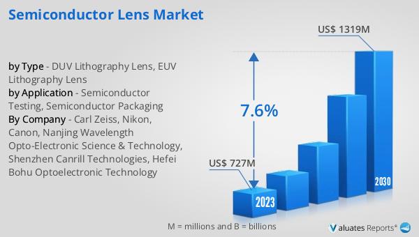
The global semiconductor lens market was valued at approximately $727 million in 2023 and is projected to grow significantly, reaching an estimated $1,319 million by 2030. This growth represents a compound annual growth rate (CAGR) of 7.6% over the forecast period from 2024 to 2030. The increasing demand for advanced semiconductor devices, driven by the proliferation of technologies such as artificial intelligence, the Internet of Things (IoT), and 5G connectivity, is a key factor contributing to this market expansion. Semiconductor lenses are essential components in the photolithography process, which is critical for the production of integrated circuits. As the semiconductor industry continues to push the boundaries of miniaturization and performance, the need for high-quality lenses that can support advanced manufacturing techniques is becoming increasingly important. The transition from DUV to EUV lithography, in particular, is expected to drive significant growth in the semiconductor lens market, as EUV lenses offer superior resolution and patterning capabilities. Additionally, the growing complexity of semiconductor devices and the increasing demand for high-precision testing and packaging solutions are further fueling the need for advanced lenses. Overall, the global semiconductor lens market is poised for robust growth, driven by technological advancements and the ever-increasing demand for sophisticated electronic devices.
| Report Metric | Details |
| Report Name | Semiconductor Lens Market |
| Accounted market size in 2023 | US$ 727 million |
| Forecasted market size in 2030 | US$ 1319 million |
| CAGR | 7.6% |
| Base Year | 2023 |
| Forecasted years | 2024 - 2030 |
| by Type |
|
| by Application |
|
| Production by Region |
|
| Consumption by Region |
|
| By Company | Carl Zeiss, Nikon, Canon, Nanjing Wavelength Opto-Electronic Science & Technology, Shenzhen Canrill Technologies, Hefei Bohu Optoelectronic Technology |
| Forecast units | USD million in value |
| Report coverage | Revenue and volume forecast, company share, competitive landscape, growth factors and trends |


