What is Global Semiconductor Packaging Mold Market?
The Global Semiconductor Packaging Mold Market is a crucial segment within the semiconductor industry, focusing on the encapsulation of semiconductor devices to protect them from physical damage, corrosion, and to ensure reliable electrical performance. This market is pivotal in the production of semiconductor devices, as the packaging mold used directly impacts the efficiency, durability, and performance of the semiconductor. The process involves encasing the semiconductor device in a protective material, typically plastic or ceramic, to safeguard the delicate internal components from environmental stress and to facilitate electrical connections. As semiconductors continue to be integral in various applications ranging from consumer electronics to automotive and industrial systems, the demand for innovative and efficient packaging solutions is on the rise. This market's growth is driven by the increasing complexity of semiconductor devices, the need for higher performance and reliability, and the ongoing miniaturization of electronic devices. The development of advanced packaging technologies, including 3D packaging and wafer-level packaging, further underscores the importance of the semiconductor packaging mold market in enabling the next generation of electronic devices.
Transfer Molds, Compression Molds in the Global Semiconductor Packaging Mold Market:
In the realm of the Global Semiconductor Packaging Mold Market, Transfer Molds and Compression Molds stand out as pivotal technologies shaping the industry. Transfer Molding is a process where pre-measured, heated resin is transferred under pressure into a mold cavity where it encapsulates the semiconductor device. This method is highly valued for its ability to produce complex shapes with excellent dimensional accuracy and fine detail, making it ideal for high-volume production of semiconductor packages. It offers a balanced mix of productivity and quality, with relatively low waste and efficient use of materials. On the other hand, Compression Molding involves placing a semiconductor device within a mold cavity and then applying heat and pressure to shape the molding compound around the device. This technique is renowned for its cost-effectiveness and the ability to produce large, complex parts with high material strength. Compression Molding is particularly suited for creating packages that require high reliability and robustness, such as those used in automotive and industrial applications. Both methods play critical roles in the semiconductor packaging process, each offering unique advantages that cater to different requirements in terms of precision, material properties, and production efficiency. As the semiconductor industry continues to evolve, the demand for sophisticated packaging solutions escalates, highlighting the significance of Transfer and Compression Molding technologies in enabling the development of advanced semiconductor devices.
WLP, PSP, Others in the Global Semiconductor Packaging Mold Market:
The Global Semiconductor Packaging Mold Market finds its applications sprawling across various domains, notably in Wafer Level Packaging (WLP), Panel Size Packaging (PSP), and others. WLP is a cutting-edge technology that involves packaging the semiconductor device at the wafer level, significantly reducing the size and cost of the package. This method enhances the electrical performance of the device and is particularly beneficial for applications where space and weight are critical factors, such as in mobile devices and wearable technology. PSP, on the other hand, represents a shift towards larger panel sizes for packaging, allowing for more devices to be processed simultaneously, thereby increasing throughput and reducing costs. This approach is gaining traction in the industry, especially for the production of large volumes of semiconductor devices, as it offers economies of scale. Other areas of application include traditional and advanced packaging technologies that cater to specific needs of the semiconductor devices, such as thermal management, integration of different semiconductor technologies (e.g., MEMS, sensors), and enhancement of the device's mechanical and electrical performance. The versatility and adaptability of the Global Semiconductor Packaging Mold Market to the evolving requirements of the semiconductor industry underscore its critical role in enabling the next generation of electronic devices across a myriad of applications.
Global Semiconductor Packaging Mold Market Outlook:
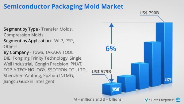
The market outlook for the global semiconductor industry presents a promising trajectory, with the valuation estimated at US$ 579 billion in 2022, and projections indicating a rise to US$ 790 billion by 2029. This growth, expected to occur at a Compound Annual Growth Rate (CAGR) of 6% during the forecast period, underscores the dynamic and expanding nature of the semiconductor sector. The industry's growth is fueled by the relentless demand for semiconductor devices across various applications, including consumer electronics, automotive, and industrial systems. As technologies continue to advance, the need for more sophisticated, efficient, and miniaturized semiconductor components escalates, driving the market forward. This upward trend reflects the critical role of semiconductors in the modern digital economy, powering everything from smartphones and computers to advanced driver-assistance systems (ADAS) and Internet of Things (IoT) devices. The projected growth not only highlights the robust health of the semiconductor industry but also points to the continuous innovation and development efforts aimed at meeting the ever-increasing demands of technology consumers and industries worldwide.
| Report Metric | Details |
| Report Name | Semiconductor Packaging Mold Market |
| Accounted market size in year | US$ 579 billion |
| Forecasted market size in 2029 | US$ 790 billion |
| CAGR | 6% |
| Base Year | year |
| Forecasted years | 2024 - 2029 |
| Segment by Type |
|
| Segment by Application |
|
| Production by Region |
|
| Consumption by Region |
|
| By Company | Towa, TAKARA TOOL & DIE, Tongling Trinity Technology, Single Well Industrial, Gongin Precision, PNAT, TOP-A TECHNOLOGY, SSOTRON CO., LTD, Shenzhen Yaotong, Suzhou INTMG, Jiangsu Guoxin Intelligent |
| Forecast units | USD million in value |
| Report coverage | Revenue and volume forecast, company share, competitive landscape, growth factors and trends |


