Friday, January 3, 2025

Ultra-High Purity Metal Sputtering Targets - Global Market Share and Ranking, Overall Sales and Demand Forecast 2024-2030

What is Ultra-High Purity Metal Sputtering Targets - Global Market?

Ultra-high purity metal sputtering targets are essential components in the manufacturing processes of various high-tech industries. These targets are made from metals that have been refined to an extremely high level of purity, often exceeding 99.99%. This high purity is crucial because it ensures that the thin films deposited during the sputtering process are free from impurities that could affect the performance of the final product. The global market for these sputtering targets is driven by the increasing demand for advanced electronic devices, solar panels, and other high-tech applications. As technology continues to advance, the need for materials that can deliver superior performance and reliability becomes more critical. This demand is reflected in the growing market for ultra-high purity metal sputtering targets, which are used in the production of semiconductors, flat panel displays, and other electronic components. The market is characterized by a high level of competition, with numerous manufacturers striving to produce targets that meet the stringent quality standards required by their customers.

Ultra-High Purity Metal Sputtering Targets - Market

Aluminum Sputtering Target, Titanium Sputtering Target, Copper Sputtering Target, Tantalum Sputtering Target, Tungsten Sputtering Target, Molybdenum Sputtering Target, Others in the Ultra-High Purity Metal Sputtering Targets - Global Market:

Aluminum sputtering targets are widely used in the electronics industry due to their excellent conductivity and corrosion resistance. These targets are essential in the production of thin films for semiconductors and flat panel displays. The demand for aluminum sputtering targets is driven by the increasing production of electronic devices and the need for efficient and reliable materials. Titanium sputtering targets, on the other hand, are known for their high strength and resistance to corrosion. They are commonly used in the aerospace and medical industries, where durability and reliability are paramount. The use of titanium sputtering targets in the production of medical implants and aerospace components is a testament to their versatility and performance. Copper sputtering targets are highly valued for their excellent electrical conductivity and thermal properties. They are widely used in the production of printed circuit boards and other electronic components. The demand for copper sputtering targets is closely linked to the growth of the electronics industry and the increasing need for high-performance materials. Tantalum sputtering targets are known for their high melting point and excellent corrosion resistance. They are used in the production of capacitors and other electronic components that require materials that can withstand extreme conditions. The demand for tantalum sputtering targets is driven by the need for reliable and durable materials in the electronics industry. Tungsten sputtering targets are valued for their high density and melting point. They are used in the production of X-ray tubes and other high-temperature applications. The demand for tungsten sputtering targets is driven by the need for materials that can withstand extreme temperatures and provide reliable performance. Molybdenum sputtering targets are known for their excellent thermal and electrical conductivity. They are used in the production of thin films for solar panels and other electronic components. The demand for molybdenum sputtering targets is closely linked to the growth of the solar energy industry and the increasing need for efficient and reliable materials. Other sputtering targets, such as those made from nickel, cobalt, and other metals, are also used in various high-tech applications. The demand for these targets is driven by the need for materials that can deliver superior performance and reliability in a wide range of applications.

Semiconductor, Solar Photovoltaic, Others in the Ultra-High Purity Metal Sputtering Targets - Global Market:

Ultra-high purity metal sputtering targets play a crucial role in the semiconductor industry, where they are used to deposit thin films on silicon wafers. These thin films are essential for the production of integrated circuits and other semiconductor devices. The demand for ultra-high purity metal sputtering targets in the semiconductor industry is driven by the increasing complexity of electronic devices and the need for materials that can deliver superior performance and reliability. In the solar photovoltaic industry, ultra-high purity metal sputtering targets are used to deposit thin films on solar cells. These thin films are essential for improving the efficiency and performance of solar panels. The demand for ultra-high purity metal sputtering targets in the solar photovoltaic industry is driven by the increasing adoption of solar energy and the need for materials that can deliver superior performance and reliability. In addition to the semiconductor and solar photovoltaic industries, ultra-high purity metal sputtering targets are also used in a wide range of other applications. These include the production of flat panel displays, optical coatings, and other high-tech products. The demand for ultra-high purity metal sputtering targets in these applications is driven by the need for materials that can deliver superior performance and reliability in a wide range of applications. As technology continues to advance, the demand for ultra-high purity metal sputtering targets is expected to grow, driven by the increasing need for materials that can deliver superior performance and reliability in a wide range of applications.

Ultra-High Purity Metal Sputtering Targets - Global Market Outlook:

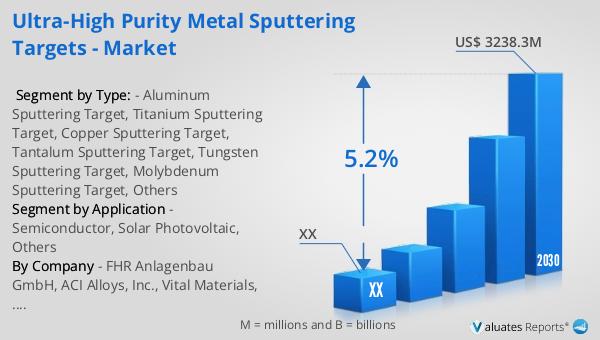
The global market for ultra-high purity metal sputtering targets was valued at approximately $2,248 million in 2023. It is projected to grow to a revised size of around $3,238.3 million by 2030, reflecting a compound annual growth rate (CAGR) of 5.2% during the forecast period from 2024 to 2030. This growth is indicative of the increasing demand for high-purity materials in various high-tech industries, including electronics, solar energy, and others. The North American market for these sputtering targets was also valued at a significant amount in 2023, with expectations of reaching a higher value by 2030, although specific figures are not provided. The growth in this region is expected to align with the global trend, driven by advancements in technology and the increasing need for reliable and efficient materials. The market outlook suggests a positive trajectory for ultra-high purity metal sputtering targets, underscoring their importance in the production of advanced electronic devices and other high-tech applications. As industries continue to evolve and demand more sophisticated materials, the market for these sputtering targets is poised for significant growth.


Report Metric Details
Report Name Ultra-High Purity Metal Sputtering Targets - Market
Forecasted market size in 2030 US$ 3238.3 million
CAGR 5.2%
Forecasted years 2024 - 2030
Segment by Type:
  • Aluminum Sputtering Target
  • Titanium Sputtering Target
  • Copper Sputtering Target
  • Tantalum Sputtering Target
  • Tungsten Sputtering Target
  • Molybdenum Sputtering Target
  • Others
Segment by Application
  • Semiconductor
  • Solar Photovoltaic
  • Others
By Region
  • North America (United States, Canada)
  • Europe (Germany, France, UK, Italy, Russia) Rest of Europe
  • Nordic Countries
  • Asia-Pacific (China, Japan, South Korea)
  • Southeast Asia (India, Australia)
  • Rest of Asia
  • Latin America (Mexico, Brazil)
  • Rest of Latin America
  • Middle East & Africa (Turkey, Saudi Arabia, UAE, Rest of MEA)
By Company FHR Anlagenbau GmbH, ACI Alloys, Inc., Vital Materials, Matsurf Technologies Inc, Plasmaterials, Inc., Creative Semiconductor Engineering, Sputtering Target and Evaporation Material, American Elements, AEM, CHINA RARE METAL MATERLAL CO.,LTD., Changsha Xinkang Advanced Materials Co.,Ltd, JX Nippon Mining & Metals Corporation, Plansee SE, Praxair, Honeywell, ULVAC, Hitachi Metals
Forecast units USD million in value
Report coverage Revenue and volume forecast, company share, competitive landscape, growth factors and trends

Zinc Selenide Raw Material - Global Market Share and Ranking, Overall Sales and Demand Forecast 2024-2030

What is Zinc Selenide Raw Material - Global Market?

Zinc Selenide (ZnSe) is a chemical compound that plays a crucial role in various industries due to its unique properties. It is primarily used as a raw material in the global market for applications that require high optical transparency and thermal resistance. ZnSe is a yellowish, crystalline solid that is known for its ability to transmit infrared light, making it an essential component in optical devices. The global market for Zinc Selenide raw material is driven by its demand in sectors such as electronics, semiconductors, medical fields, and thermal imaging systems. Its ability to withstand high temperatures and its non-reactive nature make it suitable for use in harsh environments. The market is characterized by a steady demand due to its applications in cutting-edge technologies and industries that require precision and reliability. As industries continue to innovate and develop new technologies, the demand for Zinc Selenide is expected to grow, further solidifying its position as a vital raw material in the global market. The versatility and efficiency of ZnSe in various applications underscore its importance and ensure its continued relevance in the market.

Zinc Selenide Raw Material - Market

<50mm, 50-150mm, 150-250mm, Above 250mm in the Zinc Selenide Raw Material - Global Market:

Zinc Selenide raw material is available in various sizes, each catering to specific applications and industries. The size categories include <50mm, 50-150mm, 150-250mm, and above 250mm, each offering distinct advantages and uses. The <50mm size is typically used in applications where precision and compactness are crucial. This size is ideal for small-scale optical devices and components that require high accuracy and minimal space. The 50-150mm size range is more versatile, often used in medium-sized optical systems and devices. It provides a balance between size and performance, making it suitable for a wide range of applications, including some medical devices and imaging systems. The 150-250mm size is generally used in larger systems where more substantial components are necessary. This size is often found in industrial applications and larger optical systems that require robust and durable materials. Finally, the above 250mm size category is used in specialized applications that demand large-scale components. These are typically found in industrial and research settings where the size and durability of the material are critical. Each size category of Zinc Selenide raw material offers unique benefits, allowing it to be tailored to specific needs and applications across various industries. The availability of different sizes ensures that Zinc Selenide can meet the diverse requirements of its users, from small-scale precision devices to large industrial systems. This adaptability is one of the key factors driving the demand for Zinc Selenide in the global market. As technology continues to advance, the need for materials that can be customized to specific applications will only increase, further highlighting the importance of Zinc Selenide in the market. The ability to choose from a range of sizes allows manufacturers and developers to optimize their products and systems, ensuring that they meet the highest standards of performance and reliability. This flexibility is crucial in industries where precision and efficiency are paramount, and Zinc Selenide's ability to deliver on these fronts makes it an indispensable material in the global market.

Electronics and Semiconductors, Medical Field, Thermal Imaging System, Others in the Zinc Selenide Raw Material - Global Market:

Zinc Selenide raw material is widely used in various fields due to its exceptional properties, particularly in electronics and semiconductors, the medical field, thermal imaging systems, and other applications. In the electronics and semiconductor industry, ZnSe is valued for its optical properties and thermal stability. It is used in the production of laser diodes, optical windows, and lenses, where its ability to transmit infrared light is crucial. The material's high resistance to thermal shock and its non-reactive nature make it ideal for use in environments where precision and reliability are essential. In the medical field, Zinc Selenide is used in imaging systems and diagnostic equipment. Its ability to provide clear and accurate imaging makes it a valuable component in medical devices that require high precision and reliability. The material's non-toxic nature also makes it suitable for use in medical applications where safety is a priority. In thermal imaging systems, ZnSe is used for its ability to transmit infrared light, which is essential for capturing thermal images. This makes it a critical component in systems used for surveillance, security, and industrial inspections. The material's durability and resistance to harsh environments make it ideal for use in these demanding applications. Beyond these specific fields, Zinc Selenide is also used in other applications that require high optical clarity and thermal resistance. Its versatility and efficiency make it a popular choice for a wide range of industries, from aerospace to telecommunications. The material's ability to meet the diverse needs of these industries underscores its importance in the global market. As technology continues to evolve, the demand for materials like Zinc Selenide that can deliver high performance and reliability will only increase, further solidifying its position as a key raw material in the global market.

Zinc Selenide Raw Material - Global Market Outlook:

The global market for Zinc Selenide raw material was valued at approximately $1,798 million in 2023. Looking ahead, it is projected to grow to a revised size of about $2,219.5 million by the year 2030. This growth represents a compound annual growth rate (CAGR) of 3.1% over the forecast period from 2024 to 2030. This steady growth rate indicates a consistent demand for Zinc Selenide across various industries, driven by its unique properties and wide range of applications. The market's expansion is likely fueled by the increasing need for advanced materials in sectors such as electronics, semiconductors, and medical devices, where precision and reliability are paramount. As industries continue to innovate and develop new technologies, the demand for materials like Zinc Selenide that can meet these evolving needs is expected to rise. This growth trajectory highlights the importance of Zinc Selenide as a critical raw material in the global market, with its ability to deliver high performance and adaptability to various applications ensuring its continued relevance and demand. The projected increase in market size reflects the ongoing advancements in technology and the growing need for materials that can support these innovations, making Zinc Selenide an indispensable component in the global market landscape.


Report Metric Details
Report Name Zinc Selenide Raw Material - Market
Forecasted market size in 2030 US$ 2219.5 million
CAGR 3.1%
Forecasted years 2024 - 2030
Segment by Type:
  • <50mm
  • 50-150mm
  • 150-250mm
  • Above 250mm
Segment by Application
  • Electronics and Semiconductors
  • Medical Field
  • Thermal Imaging System
  • Others
By Region
  • North America (United States, Canada)
  • Europe (Germany, France, UK, Italy, Russia) Rest of Europe
  • Nordic Countries
  • Asia-Pacific (China, Japan, South Korea)
  • Southeast Asia (India, Australia)
  • Rest of Asia
  • Latin America (Mexico, Brazil)
  • Rest of Latin America
  • Middle East & Africa (Turkey, Saudi Arabia, UAE, Rest of MEA)
By Company American Elements, Vital Materials, EdgeTech Industries, LLC, II-VI Incorporated, Noah Chemicals, EO, TYBANG, R'AIN Group, Crystaltechno, Alkor Technologies, Wavelength-tech, Altechna, EKSMA Optics
Forecast units USD million in value
Report coverage Revenue and volume forecast, company share, competitive landscape, growth factors and trends

Zinc Sulfide Raw Material - Global Market Share and Ranking, Overall Sales and Demand Forecast 2024-2030

What is Zinc Sulfide Raw Material - Global Market?

Zinc sulfide is a versatile raw material that plays a significant role in various industries worldwide. It is a chemical compound with the formula ZnS and is primarily used in the production of phosphors, pigments, and optical materials. The global market for zinc sulfide raw material is driven by its extensive applications in different sectors, including electronics, optics, and coatings. This compound is known for its excellent luminescent properties, making it a popular choice in the manufacturing of display screens, X-ray screens, and other optical devices. Additionally, zinc sulfide is used as a pigment in paints and plastics due to its ability to provide a bright white color. The demand for zinc sulfide is also fueled by its use in the semiconductor industry, where it serves as a crucial component in the production of various electronic devices. As industries continue to innovate and expand, the global market for zinc sulfide raw material is expected to grow, driven by its diverse applications and the increasing demand for advanced materials.

Zinc Sulfide Raw Material - Market

in the Zinc Sulfide Raw Material - Global Market:

Zinc sulfide raw material is utilized in various forms to cater to the diverse needs of different customers across the global market. One of the primary forms of zinc sulfide is its use as a phosphor material. Phosphors are substances that exhibit the phenomenon of luminescence, and zinc sulfide is widely used in this capacity due to its ability to emit light when exposed to ultraviolet or electron beam excitation. This property makes it an essential component in the production of cathode ray tubes, electroluminescent panels, and other display technologies. Another significant form of zinc sulfide is its use as a pigment. In this application, zinc sulfide is valued for its bright white color and is often used in combination with other pigments to enhance the opacity and brightness of paints, coatings, and plastics. This makes it a popular choice in the automotive, construction, and consumer goods industries, where high-quality finishes are required. Additionally, zinc sulfide is used in the production of optical materials. Its high refractive index and transparency in the infrared spectrum make it suitable for use in lenses, windows, and other optical components. This is particularly important in the defense and aerospace industries, where advanced optical systems are required for targeting, surveillance, and navigation. Furthermore, zinc sulfide is used in the semiconductor industry, where it serves as a crucial material in the fabrication of electronic devices. Its properties as a wide bandgap semiconductor make it suitable for use in light-emitting diodes (LEDs), laser diodes, and other optoelectronic devices. The versatility of zinc sulfide raw material and its ability to meet the specific needs of various industries make it a valuable commodity in the global market. As technology continues to advance and new applications for zinc sulfide are discovered, its demand is expected to grow, further solidifying its position as a key material in multiple sectors.

Semiconductor, Optical Applications, Others in the Zinc Sulfide Raw Material - Global Market:

Zinc sulfide raw material finds extensive usage in several key areas, including semiconductors, optical applications, and other industries. In the semiconductor sector, zinc sulfide is valued for its properties as a wide bandgap semiconductor. This makes it an ideal material for the production of light-emitting diodes (LEDs), laser diodes, and other optoelectronic devices. The ability of zinc sulfide to efficiently emit light when subjected to electrical excitation is crucial in the development of energy-efficient lighting solutions and advanced display technologies. Its role in the semiconductor industry is further enhanced by its compatibility with other semiconductor materials, allowing for the creation of complex electronic devices with improved performance and reliability. In optical applications, zinc sulfide is prized for its high refractive index and excellent transparency in the infrared spectrum. These properties make it an essential material in the production of lenses, windows, and other optical components used in a variety of industries. In the defense and aerospace sectors, zinc sulfide is used in the manufacturing of advanced optical systems for targeting, surveillance, and navigation. Its ability to withstand harsh environmental conditions and provide clear, high-quality images is critical in these applications. Additionally, zinc sulfide is used in the production of infrared optics for thermal imaging cameras, which are widely used in security, firefighting, and industrial inspection. Beyond semiconductors and optical applications, zinc sulfide is also utilized in other industries due to its unique properties. In the coatings industry, it is used as a pigment to provide a bright white color and enhance the opacity of paints and coatings. This makes it a popular choice in the automotive and construction industries, where high-quality finishes are required. Furthermore, zinc sulfide is used in the production of phosphors for cathode ray tubes, electroluminescent panels, and other display technologies. Its ability to emit light when exposed to ultraviolet or electron beam excitation makes it an essential component in these applications. The diverse range of uses for zinc sulfide raw material highlights its importance in the global market and underscores the need for continued research and development to explore new applications and improve existing technologies.

Zinc Sulfide Raw Material - Global Market Outlook:

The global market for zinc sulfide raw material was valued at approximately $159 million in 2023. It is projected to grow to a revised size of around $192.7 million by 2030, reflecting a compound annual growth rate (CAGR) of 2.7% during the forecast period from 2024 to 2030. This growth is indicative of the increasing demand for zinc sulfide across various industries, driven by its versatile applications and unique properties. In North America, the market for zinc sulfide raw material was valued at a certain amount in 2023 and is expected to reach a specific value by 2030, with a CAGR of a certain percentage during the forecast period. The growth in the North American market is likely to be influenced by the region's strong industrial base and the presence of key players in the electronics, optics, and coatings industries. The steady growth of the zinc sulfide market globally and in North America highlights the material's significance in various sectors and the ongoing demand for advanced materials that can meet the evolving needs of modern industries. As the market continues to expand, companies involved in the production and distribution of zinc sulfide raw material are expected to benefit from the increasing opportunities and the growing emphasis on innovation and sustainability.


Report Metric Details
Report Name Zinc Sulfide Raw Material - Market
Forecasted market size in 2030 US$ 192.7 million
CAGR 2.7%
Forecasted years 2024 - 2030
Segment by Purity:
  • 97%-99.9%
  • 99.9%-99.99%
  • ≥99.99%
Segment by Application
  • Semiconductor
  • Optical Applications
  • Others
By Region
  • North America (United States, Canada)
  • Europe (Germany, France, UK, Italy, Russia) Rest of Europe
  • Nordic Countries
  • Asia-Pacific (China, Japan, South Korea)
  • Southeast Asia (India, Australia)
  • Rest of Asia
  • Latin America (Mexico, Brazil)
  • Rest of Latin America
  • Middle East & Africa (Turkey, Saudi Arabia, UAE, Rest of MEA)
By Company Triveni Interchem, Shanghai Jing Lian, II-VI Incorporated, Reade, American Elements, Zhangjiagang Alpson, DuPont, Weifang Sunny, Vital Materials, Wuhan Xinrong, Venator Materials PLC., PIDC, Leshan Kaiyada
Forecast units USD million in value
Report coverage Revenue and volume forecast, company share, competitive landscape, growth factors and trends

Infrared Thermal Imager - Global Market Share and Ranking, Overall Sales and Demand Forecast 2024-2030

What is Infrared Thermal Imager - Global Market?

Infrared thermal imagers are sophisticated devices that capture and convert infrared radiation into visible images, allowing users to see temperature variations across surfaces. These devices are pivotal in various industries due to their ability to detect heat patterns and anomalies that are invisible to the naked eye. The global market for infrared thermal imagers is expanding as industries increasingly recognize their value in enhancing safety, efficiency, and diagnostics. These imagers are used in applications ranging from electrical inspections to medical diagnostics, where they help identify issues like overheating components or inflammation in the human body. The market's growth is driven by technological advancements, increasing demand for predictive maintenance, and the rising need for non-invasive diagnostic tools. As industries continue to innovate and integrate these devices into their operations, the demand for infrared thermal imagers is expected to rise, reflecting their critical role in modern technology and safety protocols.

Infrared Thermal Imager - Market

Shortwave Infrared, Medium Wave Infrared, Long Wave Infrared in the Infrared Thermal Imager - Global Market:

Infrared thermal imagers operate across different wavelengths, each offering unique advantages and applications. Shortwave infrared (SWIR) imagers typically operate in the 0.9 to 1.7 micrometer range. They are particularly useful in applications where visible light is limited, such as night vision and surveillance. SWIR imagers can penetrate through smoke, fog, and other obscurants, making them invaluable in military and security operations. They are also used in industrial settings for quality control and process monitoring, as they can detect moisture content and other material properties that are not visible in other wavelengths. Medium wave infrared (MWIR) imagers, operating in the 3 to 5 micrometer range, are known for their high sensitivity and resolution. They are ideal for applications requiring precise temperature measurements, such as in scientific research and aerospace. MWIR imagers are also used in environmental monitoring, where they help track changes in temperature and detect gas leaks. Long wave infrared (LWIR) imagers, which operate in the 8 to 14 micrometer range, are the most common type of thermal imagers. They are widely used in building inspections, firefighting, and automotive applications due to their ability to detect heat loss, identify electrical faults, and enhance driver safety. LWIR imagers are also used in medical diagnostics, where they help detect inflammation and other heat-related anomalies in the human body. Each of these infrared bands offers distinct advantages, making them suitable for a wide range of applications across different industries. As technology continues to advance, the capabilities of infrared thermal imagers are expected to expand, further enhancing their utility and market demand.

Electricity, Medical, Aerospace, Automotive, Others in the Infrared Thermal Imager - Global Market:

Infrared thermal imagers have a wide range of applications across various industries, each leveraging the technology's ability to detect and visualize heat patterns. In the electricity sector, these devices are used for inspecting electrical systems and components. They help identify overheating components, loose connections, and other potential issues that could lead to equipment failure or fire hazards. By enabling early detection, thermal imagers contribute to preventive maintenance and enhance the safety and reliability of electrical systems. In the medical field, infrared thermal imagers are used for non-invasive diagnostics. They help detect inflammation, circulatory issues, and other conditions by visualizing heat patterns on the skin. This technology is particularly useful in identifying areas of concern without the need for direct contact or radiation exposure. In the aerospace industry, thermal imagers are used for inspecting aircraft components and systems. They help detect heat-related issues, such as overheating engines or faulty insulation, which could compromise safety and performance. In the automotive industry, infrared thermal imagers are used for vehicle diagnostics and safety enhancements. They help identify issues like overheating engines, brake problems, and tire defects, contributing to vehicle maintenance and safety. Additionally, thermal imagers are used in driver assistance systems to enhance visibility in low-light conditions. Beyond these industries, infrared thermal imagers are used in various other applications, such as building inspections, firefighting, and environmental monitoring. They help detect heat loss, identify fire hotspots, and monitor temperature changes in the environment. The versatility and effectiveness of infrared thermal imagers make them indispensable tools in many fields, driving their demand and market growth.

Infrared Thermal Imager - Global Market Outlook:

The global market for infrared thermal imagers was valued at approximately $4,435 million in 2023. It is projected to grow to a revised size of around $5,650.8 million by 2030, with a compound annual growth rate (CAGR) of 3.4% during the forecast period from 2024 to 2030. This growth is driven by the increasing adoption of thermal imaging technology across various industries, including electrical, medical, aerospace, and automotive sectors. Key players in the global thermal imaging camera market include FLIR Systems Inc., L3Harris Technologies Inc., Lockheed Martin, Thales Group, and GUIDE INFRARED, among others. These top five manufacturers collectively hold a production share of over 40%, highlighting their significant influence in the market. As these companies continue to innovate and expand their product offerings, the market for infrared thermal imagers is expected to grow, driven by the increasing demand for advanced imaging solutions across different industries. The market's growth reflects the critical role that infrared thermal imagers play in enhancing safety, efficiency, and diagnostics in various applications.


Report Metric Details
Report Name Infrared Thermal Imager - Market
Forecasted market size in 2030 US$ 5650.8 million
CAGR 3.4%
Forecasted years 2024 - 2030
Segment by Type:
  • Shortwave Infrared
  • Medium Wave Infrared
  • Long Wave Infrared
Segment by Application
  • Electricity
  • Medical
  • Aerospace
  • Automotive
  • Others
By Region
  • North America (United States, Canada)
  • Europe (Germany, France, UK, Italy, Russia) Rest of Europe
  • Nordic Countries
  • Asia-Pacific (China, Japan, South Korea)
  • Southeast Asia (India, Australia)
  • Rest of Asia
  • Latin America (Mexico, Brazil)
  • Rest of Latin America
  • Middle East & Africa (Turkey, Saudi Arabia, UAE, Rest of MEA)
By Company Kollsman, FLIR, BOSCH, Fluke, Multiple PIMS, Bullard, Lynred, Jenoptics, L3 Technologies, MSA, NACHI, Teledyne, NEC, ISG, ULIS
Forecast units USD million in value
Report coverage Revenue and volume forecast, company share, competitive landscape, growth factors and trends

Gold Evaporation Materials - Global Market Share and Ranking, Overall Sales and Demand Forecast 2024-2030

What is Gold Evaporation Materials - Global Market?

Gold evaporation materials are a crucial component in various high-tech industries, primarily used in thin-film deposition processes. These materials are typically high-purity gold, which is vaporized in a vacuum chamber and then deposited onto a substrate to form a thin film. This process is essential in manufacturing semiconductors, solar cells, and other electronic devices. The global market for gold evaporation materials is driven by the increasing demand for advanced electronics and renewable energy solutions. As technology continues to evolve, the need for more efficient and reliable thin-film deposition techniques grows, further propelling the market. Additionally, the unique properties of gold, such as its excellent conductivity and resistance to oxidation, make it an ideal choice for these applications. The market is characterized by a high level of competition, with numerous players striving to develop innovative products and improve production processes to meet the growing demand. As industries continue to expand and innovate, the global market for gold evaporation materials is expected to experience significant growth, driven by technological advancements and the increasing adoption of renewable energy sources.

Gold Evaporation Materials - Market

3N, 4N, 5N, Others in the Gold Evaporation Materials - Global Market:

Gold evaporation materials are categorized based on their purity levels, commonly referred to as 3N, 4N, 5N, and others. These designations indicate the number of nines in the purity percentage of the gold used. For instance, 3N gold has a purity of 99.9%, 4N gold is 99.99% pure, and 5N gold boasts a purity of 99.999%. Each level of purity serves different applications and industries, depending on the specific requirements of the end product. 3N gold evaporation materials are typically used in applications where ultra-high purity is not critical but where the excellent conductivity and corrosion resistance of gold are still required. This level of purity is often sufficient for decorative coatings and some electronic applications where cost considerations are more significant than the need for the highest purity. 4N gold, with its higher purity, is more commonly used in the electronics and semiconductor industries, where even minor impurities can significantly affect the performance and reliability of the final product. The increased purity ensures better conductivity and fewer defects in the thin films, making it ideal for critical components in electronic devices. 5N gold evaporation materials represent the pinnacle of purity and are used in the most demanding applications, such as advanced semiconductor manufacturing and high-precision optical coatings. The near-perfect purity of 5N gold ensures the highest level of performance and reliability, which is crucial in these high-tech applications. Other purity levels, beyond 5N, are also available for specialized applications that require even greater precision and performance. These ultra-high purity materials are often used in research and development settings, where the slightest impurity could compromise the results of an experiment or the functionality of a prototype. The choice of purity level in gold evaporation materials is a critical decision that depends on the specific requirements of the application, balancing cost, performance, and reliability to achieve the desired outcome. As technology advances and the demand for high-performance materials grows, the market for gold evaporation materials across all purity levels is expected to expand, driven by the need for more efficient and reliable thin-film deposition processes.

Lighting Field, Solar Photovoltaic, Electronics and Semiconductors, Others in the Gold Evaporation Materials - Global Market:

Gold evaporation materials play a vital role in various industries, including lighting, solar photovoltaics, electronics, and semiconductors. In the lighting field, gold evaporation materials are used to create reflective coatings that enhance the efficiency and brightness of lighting devices. These coatings are applied to components such as reflectors and mirrors, improving the overall performance of lighting systems. The excellent conductivity and resistance to tarnishing of gold make it an ideal choice for these applications, ensuring long-lasting and reliable performance. In the solar photovoltaic industry, gold evaporation materials are used to create thin films that improve the efficiency of solar cells. These films enhance the electrical conductivity and light absorption properties of the cells, leading to higher energy conversion rates and more efficient solar panels. As the demand for renewable energy sources continues to grow, the use of gold evaporation materials in solar photovoltaics is expected to increase, driven by the need for more efficient and cost-effective solar solutions. In the electronics and semiconductor industries, gold evaporation materials are used to create thin films that form critical components of electronic devices. These films are used in the production of integrated circuits, sensors, and other electronic components, where the high conductivity and reliability of gold are essential. The use of gold evaporation materials in these industries is driven by the need for more advanced and reliable electronic devices, as well as the ongoing miniaturization of electronic components. Other applications of gold evaporation materials include the production of optical coatings, decorative coatings, and various research and development projects. In optical coatings, gold is used to create thin films that enhance the reflectivity and durability of optical components, such as lenses and mirrors. Decorative coatings benefit from the aesthetic appeal and durability of gold, making it a popular choice for high-end products and luxury items. In research and development, gold evaporation materials are used to create thin films for experimental purposes, where the high purity and reliability of gold are crucial for accurate results. As industries continue to innovate and expand, the use of gold evaporation materials in these and other applications is expected to grow, driven by the need for more efficient and reliable thin-film deposition processes.

Gold Evaporation Materials - Global Market Outlook:

The global market for gold evaporation materials was valued at approximately $9,021 million in 2023. It is projected to undergo a significant transformation, with an anticipated adjusted market size of around $1,838.6 million by 2030. This change reflects a compound annual growth rate (CAGR) of 10.5% during the forecast period from 2024 to 2030. The North American segment of this market was also valued at a substantial figure in 2023, with expectations of reaching a new valuation by 2030, maintaining a steady CAGR throughout the forecast period. This growth is indicative of the increasing demand for gold evaporation materials across various industries, driven by technological advancements and the rising adoption of renewable energy solutions. The market's expansion is fueled by the need for high-purity gold materials in applications such as electronics, semiconductors, and solar photovoltaics, where the unique properties of gold, including its excellent conductivity and resistance to oxidation, are highly valued. As industries continue to innovate and expand, the global market for gold evaporation materials is poised for significant growth, supported by the ongoing development of new technologies and the increasing demand for more efficient and reliable thin-film deposition processes.


Report Metric Details
Report Name Gold Evaporation Materials - Market
Forecasted market size in 2030 US$ 1838.6 million
CAGR 10.5%
Forecasted years 2024 - 2030
Segment by Type:
  • 3N
  • 4N
  • 5N
  • Others
Segment by Application
  • Lighting Field
  • Solar Photovoltaic
  • Electronics and Semiconductors
  • Others
By Region
  • North America (United States, Canada)
  • Europe (Germany, France, UK, Italy, Russia) Rest of Europe
  • Nordic Countries
  • Asia-Pacific (China, Japan, South Korea)
  • Southeast Asia (India, Australia)
  • Rest of Asia
  • Latin America (Mexico, Brazil)
  • Rest of Latin America
  • Middle East & Africa (Turkey, Saudi Arabia, UAE, Rest of MEA)
By Company STANFORD ADVANCED MATERIALS, Vacuum Engineering & Materials, Safina, AEM, Edgetech Industries, VEM, Heeger Materials Inc, American Elements, R.D. Mathis Company, Noah Chemicals, Indium Corporation
Forecast units USD million in value
Report coverage Revenue and volume forecast, company share, competitive landscape, growth factors and trends

Precision Ultrasonic Flaw Detector - Global Market Share and Ranking, Overall Sales and Demand Forecast 2024-2030

What is Precision Ultrasonic Flaw Detector - Global Market?

Precision Ultrasonic Flaw Detectors are advanced tools used in non-destructive testing to identify defects in materials without causing any damage. These devices utilize high-frequency sound waves to detect imperfections such as cracks, voids, or inclusions in a variety of materials, including metals, plastics, and composites. The global market for these detectors is expanding due to their critical role in ensuring the safety and reliability of products across various industries. They are particularly valued in sectors where material integrity is crucial, such as aerospace, automotive, and manufacturing. The precision ultrasonic flaw detector market is driven by technological advancements that enhance detection capabilities, making them more accurate and efficient. As industries continue to prioritize quality assurance and safety, the demand for these detectors is expected to grow. The market is characterized by a mix of established players and new entrants, each striving to innovate and offer more sophisticated solutions. This competitive landscape encourages continuous improvement and adaptation to meet the evolving needs of end-users. Overall, precision ultrasonic flaw detectors are indispensable tools in modern quality control processes, contributing significantly to the safety and performance of various products and structures.

Precision Ultrasonic Flaw Detector - Market

Conventional Ultrasonic Flaw Detector, Phased Array Ultrasonic Flaw Detector, TOFD Ultrasonic Flaw Detector, Others in the Precision Ultrasonic Flaw Detector - Global Market:

Conventional Ultrasonic Flaw Detectors are the traditional form of ultrasonic testing equipment. They operate by sending high-frequency sound waves into a material and analyzing the reflected waves to detect any discontinuities. These detectors are widely used due to their reliability and cost-effectiveness. They are suitable for a range of applications, from simple thickness measurements to more complex inspections of welds and castings. However, their effectiveness can be limited by the skill of the operator and the complexity of the material being tested. Phased Array Ultrasonic Flaw Detectors represent a more advanced technology. They use multiple elements in an array to steer, focus, and scan beams of sound waves, providing a more detailed and accurate image of the material being inspected. This technology allows for faster inspections and the ability to detect smaller flaws, making it ideal for critical applications in industries such as aerospace and energy. Time of Flight Diffraction (TOFD) Ultrasonic Flaw Detectors are another sophisticated option. They measure the time it takes for sound waves to travel through a material and reflect back, providing precise information about the size and location of flaws. TOFD is particularly effective for inspecting welds and is often used in conjunction with other methods to provide a comprehensive assessment. Other types of ultrasonic flaw detectors include portable and handheld devices, which offer flexibility and convenience for on-site inspections. These devices are essential for industries that require frequent testing in various locations, such as construction and maintenance. Each type of ultrasonic flaw detector has its strengths and limitations, and the choice of which to use depends on the specific requirements of the inspection task. As technology continues to evolve, these detectors are becoming more sophisticated, offering enhanced capabilities and greater ease of use. The global market for ultrasonic flaw detectors is diverse, with a range of products available to meet the needs of different industries and applications. Manufacturers are continually innovating to improve the performance and functionality of these devices, ensuring they remain an essential tool in non-destructive testing.

Industry, Manufacturing, Electronics and Semiconductors, Automotive, Others in the Precision Ultrasonic Flaw Detector - Global Market:

Precision Ultrasonic Flaw Detectors are utilized across a wide range of industries due to their ability to ensure the integrity and safety of materials and structures. In the industrial sector, these detectors are crucial for inspecting components and assemblies to detect any defects that could compromise performance or safety. They are used in the manufacturing process to ensure that products meet quality standards and are free from defects. This is particularly important in industries where safety is paramount, such as aerospace and automotive, where even minor flaws can have catastrophic consequences. In the electronics and semiconductor industries, precision ultrasonic flaw detectors are used to inspect delicate components and assemblies. These industries require high levels of precision and reliability, and ultrasonic testing provides a non-invasive method to ensure that products meet stringent quality standards. The automotive industry also relies heavily on ultrasonic flaw detectors to inspect critical components such as engine parts, transmissions, and chassis. These detectors help identify defects that could lead to failures, ensuring the safety and reliability of vehicles. In addition to these industries, precision ultrasonic flaw detectors are used in a variety of other applications, including construction, energy, and oil and gas. In construction, they are used to inspect concrete structures and welds, ensuring that buildings and infrastructure are safe and sound. In the energy sector, ultrasonic testing is used to inspect pipelines, turbines, and other critical components to prevent failures and ensure efficient operation. The oil and gas industry also relies on ultrasonic flaw detectors to inspect pipelines and other infrastructure, helping to prevent leaks and other issues that could have serious environmental and safety implications. Overall, precision ultrasonic flaw detectors are an essential tool in ensuring the safety and reliability of products and structures across a wide range of industries. Their ability to detect defects without causing damage makes them invaluable in quality control and assurance processes. As industries continue to prioritize safety and quality, the demand for these detectors is expected to grow, driving further innovation and development in the field.

Precision Ultrasonic Flaw Detector - Global Market Outlook:

The global market for Precision Ultrasonic Flaw Detectors was valued at approximately $315 million in 2023. It is projected to grow to around $400 million by 2030, with a compound annual growth rate (CAGR) of 3.4% during the forecast period from 2024 to 2030. The market is predominantly controlled by a few key players, with the top five manufacturers accounting for over 54% of the global market share. In terms of application, ultrasonic flaw detectors are most commonly used in the manufacturing and machinery sectors, which account for about 22% of the market. Other significant application areas include energy, aerospace, oil and gas, and automotive, each contributing approximately 15% to the market. This distribution highlights the widespread adoption of ultrasonic flaw detectors across various industries, driven by the need for reliable and efficient non-destructive testing solutions. As industries continue to prioritize safety and quality, the demand for precision ultrasonic flaw detectors is expected to grow, further solidifying their position as an essential tool in modern quality control processes. The competitive landscape of the market encourages continuous innovation and improvement, ensuring that these detectors remain at the forefront of non-destructive testing technology.


Report Metric Details
Report Name Precision Ultrasonic Flaw Detector - Market
Forecasted market size in 2030 US$ 400 million
CAGR 3.4%
Forecasted years 2024 - 2030
Segment by Type:
  • Conventional Ultrasonic Flaw Detector
  • Phased Array Ultrasonic Flaw Detector
  • TOFD Ultrasonic Flaw Detector
  • Others
Segment by Application
  • Industry
  • Manufacturing
  • Electronics and Semiconductors
  • Automotive
  • Others
By Region
  • North America (United States, Canada)
  • Europe (Germany, France, UK, Italy, Russia) Rest of Europe
  • Nordic Countries
  • Asia-Pacific (China, Japan, South Korea)
  • Southeast Asia (India, Australia)
  • Rest of Asia
  • Latin America (Mexico, Brazil)
  • Rest of Latin America
  • Middle East & Africa (Turkey, Saudi Arabia, UAE, Rest of MEA)
By Company Baker Hughes, NDT Systems, Advanced NDT Limited, Olympus Corporation, Screening Eagle Technologies, Elcometer, AMTEST, HUATEC Group, Sino Age Development Technology, Proceq, Beijing Cap High Technology Co.,Ltd., Beijing TIME High Technology Ltd, Jinan Hensgrand Instrument Co., Ltd, Wuxi Jiebo Electrical Technology Co., Ltd., Dragon Electronics Co, Shantou Institute of Ultrasonic Instruments Co., Ltd, ACS, Sonatest
Forecast units USD million in value
Report coverage Revenue and volume forecast, company share, competitive landscape, growth factors and trends

Composite Evaporation Material - Global Market Share and Ranking, Overall Sales and Demand Forecast 2024-2030

What is Composite Evaporation Material - Global Market?

Composite evaporation materials are specialized substances used in various industrial processes, particularly in the field of thin-film deposition. These materials are crucial in creating thin layers of material on a substrate, which is a fundamental process in manufacturing electronics, semiconductors, and other high-tech components. The global market for composite evaporation materials is driven by the increasing demand for advanced electronic devices and the need for efficient and reliable manufacturing processes. These materials are typically composed of multiple elements or compounds that are combined to achieve specific properties, such as high thermal stability, excellent adhesion, and uniform film thickness. The market is characterized by continuous innovation and development, as manufacturers strive to improve the performance and cost-effectiveness of these materials. As industries such as electronics, renewable energy, and automotive continue to grow, the demand for composite evaporation materials is expected to rise, making it a dynamic and evolving market. The global market for composite evaporation materials was valued at approximately US$ 3,216 million in 2023 and is projected to reach a size of US$ 4,655.4 million by 2030, reflecting a compound annual growth rate (CAGR) of 5.3% during the forecast period from 2024 to 2030.

Composite Evaporation Material - Market

Particles, Powder, Others in the Composite Evaporation Material - Global Market:

In the realm of composite evaporation materials, particles, powders, and other forms play a significant role in the global market. Particles are often used in the production of thin films due to their ability to provide uniform coverage and precise control over the deposition process. These particles are engineered to have specific sizes and shapes, which can influence the properties of the resulting film, such as its electrical conductivity, optical transparency, and mechanical strength. The use of particles in composite evaporation materials is particularly prevalent in the electronics and semiconductor industries, where precision and performance are paramount. Powders, on the other hand, offer a different set of advantages. They are typically used when a larger volume of material is required, or when the deposition process involves complex geometries. Powders can be easily mixed and blended to create custom compositions, allowing manufacturers to tailor the properties of the thin film to meet specific requirements. This flexibility makes powders a popular choice in industries such as photovoltaics and advanced coatings. Other forms of composite evaporation materials include granules, pellets, and liquids, each offering unique benefits depending on the application. Granules and pellets are often used in high-volume production environments, where consistency and efficiency are critical. Liquids, meanwhile, are used in processes that require a high degree of precision and control, such as atomic layer deposition. The choice of form depends on various factors, including the desired properties of the thin film, the deposition method, and the specific requirements of the application. As the global market for composite evaporation materials continues to grow, the demand for these different forms is expected to increase, driven by advancements in technology and the expanding range of applications. The versatility and adaptability of particles, powders, and other forms make them indispensable in the development of next-generation materials and technologies.

Electronics and Semiconductors, Photovoltaic Generation, Others in the Composite Evaporation Material - Global Market:

Composite evaporation materials are extensively used in various industries, with electronics and semiconductors, photovoltaic generation, and other sectors being the primary areas of application. In the electronics and semiconductor industry, these materials are crucial for the production of integrated circuits, microchips, and other components that require precise and uniform thin films. The ability to control the thickness and composition of these films is essential for ensuring the performance and reliability of electronic devices. Composite evaporation materials provide the necessary properties, such as high thermal stability and excellent adhesion, to meet the stringent requirements of this industry. In photovoltaic generation, composite evaporation materials are used to create thin-film solar cells, which are an alternative to traditional silicon-based solar cells. These materials offer several advantages, including lower production costs, flexibility, and the ability to be deposited on a variety of substrates. The use of composite evaporation materials in photovoltaic generation is driven by the growing demand for renewable energy sources and the need for more efficient and cost-effective solar technologies. Other industries that utilize composite evaporation materials include automotive, aerospace, and optics. In the automotive industry, these materials are used to create advanced coatings that improve the durability and performance of vehicle components. In aerospace, they are used in the production of lightweight and high-strength materials for aircraft and spacecraft. In optics, composite evaporation materials are used to create anti-reflective coatings and other optical components that enhance the performance of lenses and other devices. The versatility and adaptability of composite evaporation materials make them an essential component in the development of innovative technologies across a wide range of industries. As the demand for advanced materials continues to grow, the global market for composite evaporation materials is expected to expand, driven by the increasing need for high-performance and cost-effective solutions.

Composite Evaporation Material - Global Market Outlook:

The global market for composite evaporation materials was valued at approximately US$ 3,216 million in 2023 and is projected to reach a size of US$ 4,655.4 million by 2030, reflecting a compound annual growth rate (CAGR) of 5.3% during the forecast period from 2024 to 2030. This growth is indicative of the increasing demand for these materials across various industries, driven by advancements in technology and the need for more efficient and reliable manufacturing processes. In North America, the market for composite evaporation materials is also expected to grow, although specific figures for this region were not provided. The growth in North America can be attributed to the presence of a strong electronics and semiconductor industry, as well as the increasing adoption of renewable energy technologies. As industries continue to evolve and new applications for composite evaporation materials are discovered, the market is expected to experience sustained growth, offering opportunities for manufacturers and suppliers to expand their product offerings and reach new markets. The dynamic nature of the composite evaporation materials market, coupled with the ongoing advancements in technology, makes it an exciting and promising area for investment and innovation.


Report Metric Details
Report Name Composite Evaporation Material - Market
Forecasted market size in 2030 US$ 4655.4 million
CAGR 5.3%
Forecasted years 2024 - 2030
Segment by Type:
  • Particles
  • Powder
  • Others
Segment by Application
  • Electronics and Semiconductors
  • Photovoltaic Generation
  • Others
By Region
  • North America (United States, Canada)
  • Europe (Germany, France, UK, Italy, Russia) Rest of Europe
  • Nordic Countries
  • Asia-Pacific (China, Japan, South Korea)
  • Southeast Asia (India, Australia)
  • Rest of Asia
  • Latin America (Mexico, Brazil)
  • Rest of Latin America
  • Middle East & Africa (Turkey, Saudi Arabia, UAE, Rest of MEA)
By Company Merck KGaA, Aida Chemical Industries, Materion, Umicore, ULVAC, Nichia, GRIKIN Advanced Materials, Canon Optron, Vacuum Engineering and Materials Co, SAM, Heeger Materials Inc, Refining Systems
Forecast units USD million in value
Report coverage Revenue and volume forecast, company share, competitive landscape, growth factors and trends

Global Strong Cation Exchange Agarose Gel Market Research Report 2025

What is Global Strong Cation Exchange Agarose Gel Market? The Global Strong Cation Exchange Agarose Gel Market is a specialized segment wit...