What is Global Gallium Arsenide Next Generation Semiconductor Market?
The Global Gallium Arsenide (GaAs) Next Generation Semiconductor Market is a rapidly evolving sector within the broader semiconductor industry. Gallium Arsenide is a compound semiconductor material that has gained significant attention due to its superior electronic properties compared to traditional silicon-based semiconductors. GaAs semiconductors are known for their high electron mobility, which allows for faster signal transmission and greater efficiency in electronic devices. This makes them particularly valuable in applications requiring high-frequency performance, such as wireless communication and optoelectronic devices. The market for GaAs semiconductors is driven by the increasing demand for high-speed, high-performance electronic devices, as well as the growing adoption of advanced technologies like 5G and the Internet of Things (IoT). As industries continue to push the boundaries of technology, the need for more efficient and capable semiconductors like GaAs is expected to rise, positioning the Global Gallium Arsenide Next Generation Semiconductor Market as a key player in the future of electronics.
LEC Grown GaAs, VGF Grown GaAs in the Global Gallium Arsenide Next Generation Semiconductor Market:
LEC (Liquid Encapsulated Czochralski) and VGF (Vertical Gradient Freeze) are two prominent methods used in the production of Gallium Arsenide (GaAs) wafers, which are essential components in the Global Gallium Arsenide Next Generation Semiconductor Market. LEC grown GaAs is a traditional method where a GaAs crystal is grown from a melt using a seed crystal. This process involves encapsulating the melt with a liquid, typically boric oxide, to prevent the evaporation of arsenic, which is crucial for maintaining the stoichiometry of the compound. LEC grown GaAs is known for its high purity and uniformity, making it suitable for a wide range of applications, including high-frequency and high-power devices. However, the LEC method can introduce certain defects, such as dislocations, which can affect the performance of the final semiconductor product. On the other hand, VGF grown GaAs is a more advanced technique that involves the gradual cooling of a GaAs melt in a vertical orientation. This method allows for better control over the crystal growth process, resulting in wafers with fewer defects and higher structural integrity. VGF grown GaAs is particularly favored in applications where high-quality material is essential, such as in optoelectronic devices and high-speed communication systems. The choice between LEC and VGF grown GaAs often depends on the specific requirements of the application, with VGF offering advantages in terms of material quality and performance. As the demand for high-performance semiconductors continues to grow, both LEC and VGF methods are expected to play crucial roles in meeting the needs of the Global Gallium Arsenide Next Generation Semiconductor Market.
Wireless Communication, Optoelectronic Devices, Others in the Global Gallium Arsenide Next Generation Semiconductor Market:
The Global Gallium Arsenide Next Generation Semiconductor Market finds extensive usage in various areas, including wireless communication, optoelectronic devices, and other advanced technological applications. In wireless communication, GaAs semiconductors are highly valued for their ability to operate at high frequencies and deliver superior performance compared to traditional silicon-based semiconductors. This makes them ideal for use in mobile phones, satellite communication systems, and radar equipment, where high-speed data transmission and signal integrity are critical. The advent of 5G technology has further fueled the demand for GaAs semiconductors, as they are capable of supporting the high-frequency bands required for this next-generation wireless communication standard. In the realm of optoelectronic devices, GaAs semiconductors are used in the production of LEDs, laser diodes, and solar cells. Their direct bandgap property allows for efficient light emission and absorption, making them suitable for applications in lighting, displays, and energy harvesting. GaAs-based solar cells, in particular, are known for their high efficiency and are used in space applications where performance and reliability are paramount. Beyond wireless communication and optoelectronics, GaAs semiconductors are also employed in various other applications, such as in the automotive industry for advanced driver-assistance systems (ADAS) and in the defense sector for electronic warfare and surveillance systems. The versatility and superior performance of GaAs semiconductors make them a critical component in the advancement of modern technology, driving their adoption across multiple industries.
Global Gallium Arsenide Next Generation Semiconductor Market Outlook:
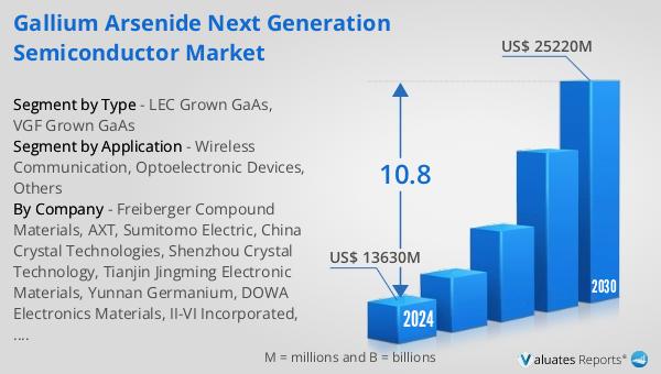
The outlook for the Global Gallium Arsenide Next Generation Semiconductor Market is promising, with projections indicating significant growth in the coming years. The market is expected to expand from $13,630 million in 2024 to $25,220 million by 2030, reflecting a robust Compound Annual Growth Rate (CAGR) of 10.8% during the forecast period. This growth is driven by the increasing demand for high-performance semiconductors in various applications, including wireless communication, optoelectronics, and other advanced technologies. The broader semiconductor market, which was valued at $579 billion in 2022, is also projected to grow, reaching $790 billion by 2029 with a CAGR of 6%. This indicates a strong overall demand for semiconductors, with GaAs playing a crucial role in meeting the needs of next-generation electronic devices. The rapid advancements in technology, coupled with the growing adoption of 5G and IoT, are expected to further drive the demand for GaAs semiconductors, positioning the Global Gallium Arsenide Next Generation Semiconductor Market as a key player in the future of the semiconductor industry.
| Report Metric | Details |
| Report Name | Gallium Arsenide Next Generation Semiconductor Market |
| Accounted market size in 2024 | US$ 13630 in million |
| Forecasted market size in 2030 | US$ 25220 million |
| CAGR | 10.8 |
| Base Year | 2024 |
| Forecasted years | 2024 - 2030 |
| Segment by Type |
|
| Segment by Application |
|
| Production by Region |
|
| Sales by Region |
|
| By Company | Freiberger Compound Materials, AXT, Sumitomo Electric, China Crystal Technologies, Shenzhou Crystal Technology, Tianjin Jingming Electronic Materials, Yunnan Germanium, DOWA Electronics Materials, II-VI Incorporated, IQE Corporation, Wafer Technology |
| Forecast units | USD million in value |
| Report coverage | Revenue and volume forecast, company share, competitive landscape, growth factors and trends |
