What is Extreme Ultraviolet (EUV) Lithography - Global Market?
Extreme Ultraviolet (EUV) Lithography is a cutting-edge technology used in the semiconductor manufacturing industry to produce extremely small and precise patterns on silicon wafers. This technology utilizes light with a wavelength of 13.5 nanometers, which is significantly shorter than the deep ultraviolet (DUV) wavelengths traditionally used in lithography. The shorter wavelength allows for the creation of smaller features on chips, which is essential for advancing Moore's Law and producing more powerful and efficient electronic devices. EUV lithography is crucial for the production of advanced microprocessors and memory chips, enabling the development of faster and more energy-efficient electronics. The global market for EUV lithography is driven by the increasing demand for high-performance computing, artificial intelligence, and the Internet of Things (IoT), which require advanced semiconductor devices. As the semiconductor industry continues to push the boundaries of miniaturization, EUV lithography is expected to play a pivotal role in meeting the technological demands of the future.
Mask, Mirrors, Light Source, Others in the Extreme Ultraviolet (EUV) Lithography - Global Market:
In the realm of Extreme Ultraviolet (EUV) Lithography, several critical components work in harmony to achieve the precision required for modern semiconductor manufacturing. The mask, often referred to as a photomask or reticle, is a key element in the lithography process. It contains the intricate patterns that need to be transferred onto the silicon wafer. Made from a substrate of quartz or glass, the mask is coated with a reflective material and a pattern-defining layer. The precision of the mask is paramount, as any defects can lead to errors in the final semiconductor product. Mirrors are another essential component in EUV lithography systems. Unlike traditional optical systems that use lenses, EUV lithography relies on a series of mirrors to focus and direct the EUV light. These mirrors are coated with multilayer materials to enhance reflectivity at the EUV wavelength. The alignment and quality of these mirrors are crucial for maintaining the accuracy and efficiency of the lithography process. The light source in EUV lithography is a sophisticated piece of technology that generates the EUV radiation required for the process. Typically, this involves a laser-produced plasma (LPP) source, where a high-powered laser is focused onto a target material, creating a plasma that emits EUV light. The stability and intensity of the light source are vital for consistent and reliable lithography performance. Other components in the EUV lithography system include the wafer stage, which precisely positions the silicon wafer during exposure, and the metrology systems that ensure the accuracy of the pattern transfer. These systems work together to achieve the high resolution and precision necessary for producing advanced semiconductor devices. The global market for EUV lithography is driven by the demand for these sophisticated components, as they are essential for the production of next-generation electronic devices.
Integrated Device Manufacturers (IDM), Foundry, Others in the Extreme Ultraviolet (EUV) Lithography - Global Market:
Extreme Ultraviolet (EUV) Lithography is increasingly being adopted by Integrated Device Manufacturers (IDMs), foundries, and other sectors within the semiconductor industry due to its ability to produce smaller and more precise semiconductor features. IDMs, which design and manufacture their own semiconductor devices, are leveraging EUV lithography to enhance their production capabilities. By adopting EUV technology, IDMs can produce more advanced chips with higher performance and lower power consumption, which is crucial for applications in high-performance computing, mobile devices, and automotive electronics. Foundries, which manufacture semiconductor devices for other companies, are also embracing EUV lithography to meet the growing demand for advanced chips. By offering EUV capabilities, foundries can attract customers looking to produce cutting-edge semiconductor products. This technology allows foundries to provide more competitive offerings, enabling their clients to develop innovative products in fields such as artificial intelligence, 5G communications, and IoT. Other sectors within the semiconductor industry, including research institutions and equipment manufacturers, are also exploring the potential of EUV lithography. Research institutions are investigating new materials and processes that can be enabled by EUV technology, while equipment manufacturers are developing the next generation of lithography tools to support the industry's transition to EUV. The adoption of EUV lithography across these sectors is driven by the need to keep pace with the rapid advancements in semiconductor technology and the increasing demand for more powerful and efficient electronic devices.
Extreme Ultraviolet (EUV) Lithography - Global Market Outlook:
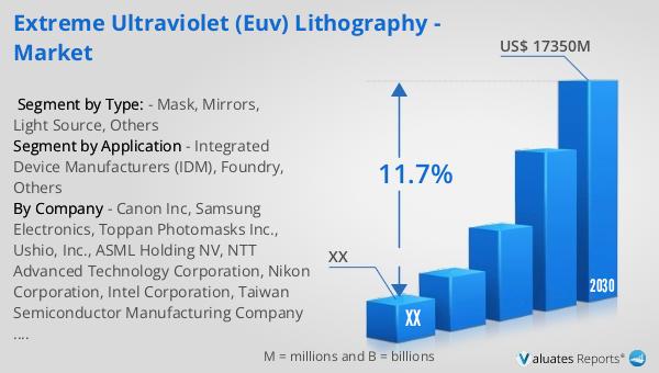
The global market for Extreme Ultraviolet (EUV) Lithography was valued at approximately $8,126 million in 2023. It is projected to grow significantly, reaching an estimated size of $17,350 million by 2030. This growth represents a compound annual growth rate (CAGR) of 11.7% during the forecast period from 2024 to 2030. The North American market is a significant contributor to this growth, driven by the presence of major semiconductor manufacturers and technological advancements in the region. The increasing demand for advanced semiconductor devices, driven by applications in high-performance computing, artificial intelligence, and the Internet of Things (IoT), is a key factor propelling the growth of the EUV lithography market. As the semiconductor industry continues to evolve, the adoption of EUV lithography is expected to expand, enabling the production of smaller, faster, and more energy-efficient chips. This growth trajectory highlights the critical role of EUV lithography in the future of semiconductor manufacturing and its potential to drive innovation across various industries.
| Report Metric | Details |
| Report Name | Extreme Ultraviolet (EUV) Lithography - Market |
| Forecasted market size in 2030 | US$ 17350 million |
| CAGR | 11.7% |
| Forecasted years | 2024 - 2030 |
| Segment by Type: |
|
| Segment by Application |
|
| By Region |
|
| By Company | Canon Inc, Samsung Electronics, Toppan Photomasks Inc., Ushio, Inc., ASML Holding NV, NTT Advanced Technology Corporation, Nikon Corporation, Intel Corporation, Taiwan Semiconductor Manufacturing Company Limited |
| Forecast units | USD million in value |
| Report coverage | Revenue and volume forecast, company share, competitive landscape, growth factors and trends |


