What is Global Silicon Wafer Testing Equipment Market?
The global Silicon Wafer Testing Equipment market is a specialized segment within the semiconductor industry that focuses on the tools and machinery used to test silicon wafers. Silicon wafers are thin slices of semiconductor material, typically silicon, which serve as the substrate for microelectronic devices. Testing equipment is crucial for ensuring the quality and reliability of these wafers before they are used in the manufacturing of integrated circuits and other semiconductor devices. The market for this equipment includes a variety of machines and technologies designed to detect defects, measure electrical properties, and ensure the overall integrity of the wafers. This market is driven by the increasing demand for high-quality semiconductors in various applications, including consumer electronics, automotive, and telecommunications. As technology advances, the need for more precise and efficient testing equipment continues to grow, making this market an essential component of the semiconductor supply chain.
Edge Detection, Surface Roughness Detection, Flatness Detection, Particle Detection in the Global Silicon Wafer Testing Equipment Market:
Edge detection, surface roughness detection, flatness detection, and particle detection are critical aspects of the global Silicon Wafer Testing Equipment market. Edge detection involves identifying the boundaries of the wafer to ensure it meets the required specifications. This process is vital for preventing issues during the subsequent manufacturing stages. Advanced imaging techniques and algorithms are employed to accurately detect and analyze the edges of the wafer. Surface roughness detection, on the other hand, focuses on measuring the texture of the wafer's surface. A smooth surface is essential for the proper functioning of semiconductor devices, as any irregularities can lead to defects in the final product. Various optical and tactile methods are used to assess surface roughness, providing detailed information about the wafer's quality. Flatness detection is another crucial aspect, as it ensures that the wafer is uniformly flat. Any deviations from flatness can cause problems during the lithography process, leading to defects in the semiconductor devices. Interferometry and other advanced techniques are used to measure the flatness of the wafer with high precision. Particle detection is equally important, as the presence of foreign particles on the wafer can lead to contamination and defects. Advanced inspection systems are used to detect and identify particles, ensuring that the wafers are clean and free from contaminants. These detection methods are integral to the overall quality control process in the semiconductor industry, helping manufacturers produce reliable and high-performance devices.
Semiconductor, Photovoltaics, Others in the Global Silicon Wafer Testing Equipment Market:
The usage of global Silicon Wafer Testing Equipment spans across various industries, including semiconductors, photovoltaics, and others. In the semiconductor industry, this equipment is essential for ensuring the quality and reliability of silicon wafers used in the production of integrated circuits and other semiconductor devices. The testing equipment helps identify defects, measure electrical properties, and ensure the overall integrity of the wafers, which is crucial for the performance and reliability of the final products. In the photovoltaics industry, silicon wafers are used as the substrate for solar cells. The testing equipment ensures that the wafers meet the required specifications and are free from defects that could affect the efficiency and performance of the solar cells. This is particularly important as the demand for renewable energy sources continues to grow, and the efficiency of solar cells plays a significant role in the overall effectiveness of solar power systems. In other industries, such as MEMS (Micro-Electro-Mechanical Systems) and LED manufacturing, silicon wafer testing equipment is used to ensure the quality and reliability of the wafers used in these applications. The equipment helps detect defects, measure surface properties, and ensure the overall integrity of the wafers, which is crucial for the performance and reliability of the final products. Overall, the usage of silicon wafer testing equipment is essential for ensuring the quality and reliability of silicon wafers across various industries, helping manufacturers produce high-performance and reliable devices.
Global Silicon Wafer Testing Equipment Market Outlook:
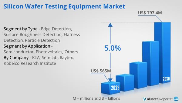
The global Silicon Wafer Testing Equipment market was valued at US$ 565 million in 2023 and is projected to reach US$ 797.4 million by 2030, reflecting a compound annual growth rate (CAGR) of 5.0% during the forecast period from 2024 to 2030. This growth is driven by the increasing demand for high-quality semiconductors in various applications, including consumer electronics, automotive, and telecommunications. As technology continues to advance, the need for more precise and efficient testing equipment becomes increasingly important, making this market an essential component of the semiconductor supply chain. The market's growth is also supported by the ongoing advancements in testing technologies, which enable manufacturers to detect defects and ensure the overall integrity of silicon wafers with greater accuracy and efficiency. This, in turn, helps improve the performance and reliability of the final semiconductor devices, meeting the growing demands of various industries.
| Report Metric | Details |
| Report Name | Silicon Wafer Testing Equipment Market |
| Accounted market size in 2023 | US$ 565 million |
| Forecasted market size in 2030 | US$ 797.4 million |
| CAGR | 5.0% |
| Base Year | 2023 |
| Forecasted years | 2024 - 2030 |
| Segment by Type |
|
| Segment by Application |
|
| Production by Region |
|
| Consumption by Region |
|
| By Company | KLA, Semilab, Raytex, Kobelco Research Institute |
| Forecast units | USD million in value |
| Report coverage | Revenue and volume forecast, company share, competitive landscape, growth factors and trends |


