What is Global Non Contact Optical Surface Profiler Market?
The Global Non-Contact Optical Surface Profiler Market refers to the industry focused on the development, production, and application of advanced instruments that measure surface topography without physical contact. These devices utilize optical techniques to create detailed 3D maps of surfaces, which are crucial for quality control, research, and development across various industries. The market encompasses a range of technologies, including white light interferometry, coherence scanning, confocal microscopy, and scanning electron microscopy with 3D reconstruction. These technologies offer high precision, non-destructive testing, and the ability to measure a wide range of surface types and materials. The demand for non-contact optical surface profilers is driven by the need for high-precision measurements in industries such as automotive, consumer electronics, and semiconductors, where surface quality and micro-scale features are critical. As technology advances and industries continue to push the boundaries of miniaturization and precision, the market for these sophisticated measurement tools is expected to grow.
White Light Interferometry, Coherence Scanning, Confocal Microscopy, Scanning Electron Microscopy (SEM) with 3D Reconstruction, Others in the Global Non Contact Optical Surface Profiler Market:
White light interferometry is a key technology in the Global Non-Contact Optical Surface Profiler Market. It uses the interference of light waves to measure surface topography with high precision. This method is particularly effective for measuring smooth surfaces and thin films. Coherence scanning, also known as coherence probe microscopy, involves scanning a surface with a coherent light source and analyzing the reflected light to create a detailed 3D image. This technique is highly effective for measuring rough surfaces and complex geometries. Confocal microscopy, another important technology, uses a focused light beam and a spatial pinhole to eliminate out-of-focus light, providing high-resolution images of surface features. This method is particularly useful for measuring surfaces with varying heights and depths. Scanning electron microscopy (SEM) with 3D reconstruction combines the high-resolution imaging capabilities of SEM with advanced software to create detailed 3D models of surfaces. This technique is invaluable for analyzing micro-scale features and materials. Other technologies in the market include laser scanning confocal microscopy and atomic force microscopy, each offering unique advantages for specific applications. These advanced measurement techniques are essential for ensuring the quality and performance of products in various industries, driving the growth of the Global Non-Contact Optical Surface Profiler Market.
Automotive Industry, Consumer Electronic, Semiconductor Industry, Others in the Global Non Contact Optical Surface Profiler Market:
The Global Non-Contact Optical Surface Profiler Market finds extensive usage in the automotive industry, where precision and surface quality are paramount. These profilers are used to measure the surface roughness, texture, and topography of various automotive components, ensuring they meet stringent quality standards. In the consumer electronics sector, non-contact optical surface profilers are crucial for the development and manufacturing of devices such as smartphones, tablets, and wearables. They help in assessing the surface quality of components like screens, lenses, and casings, which is essential for both functionality and aesthetics. The semiconductor industry also heavily relies on these profilers for the fabrication of integrated circuits and microchips. The ability to measure surface features at the micro and nano-scale is critical for ensuring the performance and reliability of semiconductor devices. Other industries, such as aerospace, medical devices, and materials science, also benefit from the precision and non-destructive testing capabilities of non-contact optical surface profilers. These instruments are used for research and development, quality control, and failure analysis, contributing to advancements in technology and product innovation. The versatility and high precision of non-contact optical surface profilers make them indispensable tools across a wide range of applications, driving their demand in the global market.
Global Non Contact Optical Surface Profiler Market Outlook:
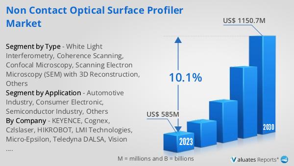
The global Non-Contact Optical Surface Profiler market was valued at US$ 585 million in 2023 and is anticipated to reach US$ 1150.7 million by 2030, witnessing a CAGR of 10.1% during the forecast period from 2024 to 2030. This significant growth reflects the increasing demand for high-precision measurement tools across various industries. As technology continues to advance, the need for accurate and non-destructive surface measurement becomes more critical, driving the adoption of non-contact optical surface profilers. These instruments offer unparalleled precision and versatility, making them essential for quality control, research, and development in sectors such as automotive, consumer electronics, and semiconductors. The market's growth is also fueled by the ongoing miniaturization of electronic components and the increasing complexity of surface features, which require advanced measurement techniques. As industries continue to push the boundaries of innovation and precision, the demand for non-contact optical surface profilers is expected to rise, contributing to the market's robust growth.
| Report Metric | Details |
| Report Name | Non Contact Optical Surface Profiler Market |
| Accounted market size in 2023 | US$ 585 million |
| Forecasted market size in 2030 | US$ 1150.7 million |
| CAGR | 10.1% |
| Base Year | 2023 |
| Forecasted years | 2024 - 2030 |
| Segment by Type |
|
| Segment by Application |
|
| Production by Region |
|
| Consumption by Region |
|
| By Company | KEYENCE, Cognex, Czlslaser, HIKROBOT, LMI Technologies, Micro-Epsilon, Teledyna DALSA, Vision Components, Qingbo Optoelectronics, SmartRay, Zebra Technologies, Bruker, Taylor Hobson, Sensofar Metrology, Zygo, KLA |
| Forecast units | USD million in value |
| Report coverage | Revenue and volume forecast, company share, competitive landscape, growth factors and trends |


