What is Global Wafer Thinning and Dicing Film Market?
The global Wafer Thinning and Dicing Film market is a specialized segment within the semiconductor industry that focuses on the production and application of films used during the wafer thinning and dicing processes. These films are essential in the manufacturing of semiconductor devices, as they provide support and protection to the delicate wafers during the thinning and dicing stages. Wafer thinning involves reducing the thickness of semiconductor wafers to improve their performance and integration into various electronic devices. Dicing, on the other hand, is the process of cutting these wafers into individual chips. The films used in these processes must exhibit high adhesion, flexibility, and resistance to chemicals and mechanical stress. The market for these films is driven by the increasing demand for smaller, more efficient electronic devices, advancements in semiconductor technology, and the growing adoption of these films in various applications such as consumer electronics, automotive, and telecommunications. The market is characterized by the presence of several key players who are continuously innovating to meet the evolving needs of the semiconductor industry.
UV Film, Non-UV Film in the Global Wafer Thinning and Dicing Film Market:
UV films and Non-UV films are two primary types of films used in the Global Wafer Thinning and Dicing Film Market. UV films are designed to be sensitive to ultraviolet light, which allows them to be easily removed after the dicing process. These films are typically used in applications where precision and cleanliness are paramount. When exposed to UV light, the adhesive properties of the film weaken, making it easier to peel off without leaving any residue on the wafer. This feature is particularly beneficial in high-precision semiconductor manufacturing, where even the smallest contamination can affect the performance of the final product. UV films are commonly used in the production of advanced microchips, sensors, and other high-tech components. Non-UV films, on the other hand, do not require exposure to ultraviolet light for removal. These films rely on mechanical or thermal methods for detachment. Non-UV films are generally more robust and can withstand harsher processing conditions compared to their UV counterparts. They are often used in applications where the wafers undergo significant mechanical stress or high-temperature processes. Non-UV films are suitable for a wide range of semiconductor applications, including power devices, MEMS (Micro-Electro-Mechanical Systems), and LED manufacturing. These films provide excellent protection and support during the wafer thinning and dicing processes, ensuring that the delicate wafers remain intact and free from damage. Both UV and Non-UV films play a crucial role in the semiconductor manufacturing process. The choice between the two depends on the specific requirements of the application, such as the type of semiconductor device being produced, the processing conditions, and the desired level of cleanliness. Manufacturers often select UV films for applications that demand high precision and minimal contamination, while Non-UV films are chosen for their durability and ability to withstand more rigorous processing environments. The continuous advancements in semiconductor technology and the increasing complexity of electronic devices drive the demand for both types of films, as they enable manufacturers to achieve higher levels of performance and reliability in their products. In summary, UV films and Non-UV films are essential components in the Global Wafer Thinning and Dicing Film Market. UV films offer the advantage of easy removal through exposure to ultraviolet light, making them ideal for high-precision applications. Non-UV films, with their robustness and ability to withstand harsh processing conditions, are suitable for a broader range of semiconductor manufacturing processes. The ongoing innovations in semiconductor technology and the growing demand for advanced electronic devices ensure the continued relevance and importance of both types of films in the industry.
Back Grinding, Wafer Dicing in the Global Wafer Thinning and Dicing Film Market:
The Global Wafer Thinning and Dicing Film Market finds significant usage in the areas of back grinding and wafer dicing. Back grinding is a crucial step in the semiconductor manufacturing process, where the thickness of the wafer is reduced to the desired level. This process is essential for producing thin and lightweight semiconductor devices that can be easily integrated into various electronic products. During back grinding, the wafer is subjected to mechanical grinding to achieve the required thickness. The use of wafer thinning films during this process provides support and protection to the wafer, preventing it from cracking or breaking under the mechanical stress. These films also help in maintaining the flatness and uniformity of the wafer, ensuring consistent quality and performance of the final product. Wafer dicing is another critical application of wafer thinning and dicing films. This process involves cutting the wafer into individual semiconductor chips, which are then used in various electronic devices. Wafer dicing requires high precision and accuracy to ensure that the chips are cut without causing any damage to the delicate structures within the wafer. The use of dicing films provides stability and support to the wafer during the cutting process, minimizing the risk of chipping or cracking. These films also help in reducing the generation of particles and debris, which can contaminate the wafer and affect the performance of the semiconductor devices. In both back grinding and wafer dicing, the choice of film is crucial to achieving the desired results. UV films are often preferred for wafer dicing due to their easy removal and minimal residue, which is essential for maintaining the cleanliness and integrity of the semiconductor chips. Non-UV films, with their robustness and ability to withstand harsh processing conditions, are commonly used in back grinding applications. The selection of the appropriate film depends on factors such as the type of semiconductor device being produced, the processing conditions, and the specific requirements of the application. The use of wafer thinning and dicing films in back grinding and wafer dicing processes offers several benefits. These films provide mechanical support and protection to the wafer, ensuring that it remains intact and free from damage during the processing stages. They also help in maintaining the flatness and uniformity of the wafer, which is crucial for achieving consistent quality and performance in the final semiconductor devices. Additionally, the use of these films helps in reducing contamination and particle generation, which can affect the performance and reliability of the semiconductor chips. In conclusion, the Global Wafer Thinning and Dicing Film Market plays a vital role in the semiconductor manufacturing process, particularly in the areas of back grinding and wafer dicing. The use of these films provides essential support and protection to the wafers, ensuring that they remain intact and free from damage during the processing stages. The choice of film, whether UV or Non-UV, depends on the specific requirements of the application and the processing conditions. The ongoing advancements in semiconductor technology and the increasing demand for high-performance electronic devices drive the continued importance and relevance of wafer thinning and dicing films in the industry.
Global Wafer Thinning and Dicing Film Market Outlook:
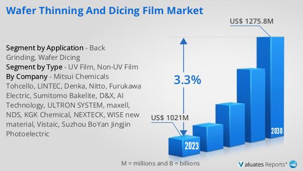
The global Wafer Thinning and Dicing Film market was valued at US$ 1021 million in 2023 and is anticipated to reach US$ 1275.8 million by 2030, witnessing a CAGR of 3.3% during the forecast period 2024-2030. The largest region, Asia Pacific, experienced a decline of 2.0 percent. Sales in the Americas were US$ 142.1 billion, up 17.0% year-on-year. Sales in Europe were US$ 53.8 billion, up 12.6% year-on-year, and sales in Japan were US$ 48.1 billion, up 10.0% year-on-year. However, sales in the largest Asia-Pacific region were US$ 336.2 billion, down 2.0% year-on-year.
| Report Metric | Details |
| Report Name | Wafer Thinning and Dicing Film Market |
| Accounted market size in 2023 | US$ 1021 million |
| Forecasted market size in 2030 | US$ 1275.8 million |
| CAGR | 3.3% |
| Base Year | 2023 |
| Forecasted years | 2024 - 2030 |
| Segment by Type |
|
| Segment by Application |
|
| Production by Region |
|
| Consumption by Region |
|
| By Company | Mitsui Chemicals Tohcello, LINTEC, Denka, Nitto, Furukawa Electric, Sumitomo Bakelite, D&X, AI Technology, ULTRON SYSTEM, maxell, NDS, KGK Chemical, NEXTECK, WISE new material, Vistaic, Suzhou BoYan Jingjin Photoelectric |
| Forecast units | USD million in value |
| Report coverage | Revenue and volume forecast, company share, competitive landscape, growth factors and trends |


