What is Global Wafer Thinning and Dicing UV Film Market?
The Global Wafer Thinning and Dicing UV Film Market is a specialized segment within the semiconductor industry that focuses on the production and application of UV films used in the wafer thinning and dicing processes. These films are essential for protecting delicate semiconductor wafers during the manufacturing process, ensuring that they remain intact and free from damage. Wafer thinning involves reducing the thickness of semiconductor wafers to improve their performance and integration into various electronic devices. Dicing, on the other hand, is the process of cutting these wafers into individual chips. UV films play a crucial role in both these processes by providing a protective layer that can be easily removed using ultraviolet light. This market is driven by the increasing demand for smaller, more efficient electronic devices, which require advanced semiconductor manufacturing techniques. The growth of the consumer electronics, automotive, and telecommunications industries further fuels the demand for wafer thinning and dicing UV films.
Back Grinding UV Film, Wafer Dicing UV Film in the Global Wafer Thinning and Dicing UV Film Market:
Back Grinding UV Film and Wafer Dicing UV Film are two critical components within the Global Wafer Thinning and Dicing UV Film Market. Back Grinding UV Film is used during the wafer thinning process, where it provides a protective layer to the wafer's surface, preventing damage and contamination. This film is designed to withstand the mechanical stress and heat generated during the grinding process, ensuring that the wafer remains intact and its surface remains smooth. Once the grinding process is complete, the UV film can be easily removed using ultraviolet light, leaving the wafer ready for further processing. Wafer Dicing UV Film, on the other hand, is used during the dicing process, where it protects the wafer from chipping and cracking as it is cut into individual chips. This film is also designed to be easily removed using UV light, ensuring that the chips remain clean and free from residue. Both types of UV films are essential for maintaining the integrity and quality of semiconductor wafers during the manufacturing process. The demand for these films is driven by the increasing complexity and miniaturization of electronic devices, which require advanced manufacturing techniques to produce high-quality semiconductor components. The growth of the consumer electronics, automotive, and telecommunications industries further fuels the demand for Back Grinding UV Film and Wafer Dicing UV Film, as these industries require smaller, more efficient electronic devices. The Global Wafer Thinning and Dicing UV Film Market is characterized by continuous innovation and development, with manufacturers constantly seeking to improve the performance and reliability of their products. This market is also highly competitive, with numerous players vying for market share by offering advanced and cost-effective solutions. The increasing adoption of advanced semiconductor manufacturing techniques, such as 3D packaging and system-in-package (SiP) technology, further drives the demand for high-quality UV films. These techniques require precise and reliable wafer thinning and dicing processes, which can only be achieved using advanced UV films. As a result, the Global Wafer Thinning and Dicing UV Film Market is expected to continue growing, driven by the increasing demand for advanced semiconductor components and the continuous development of new and improved UV film technologies.
IDMs, OSAT in the Global Wafer Thinning and Dicing UV Film Market:
The usage of Global Wafer Thinning and Dicing UV Film Market in Integrated Device Manufacturers (IDMs) and Outsourced Semiconductor Assembly and Test (OSAT) companies is crucial for the production of high-quality semiconductor components. IDMs are companies that design, manufacture, and sell their own semiconductor products. They require advanced wafer thinning and dicing processes to produce smaller, more efficient chips that can be integrated into a wide range of electronic devices. UV films play a vital role in these processes by providing a protective layer that ensures the wafers remain intact and free from damage during manufacturing. The use of UV films in wafer thinning and dicing allows IDMs to achieve the high levels of precision and reliability required for the production of advanced semiconductor components. OSAT companies, on the other hand, specialize in providing assembly, packaging, and testing services for semiconductor manufacturers. They play a critical role in the semiconductor supply chain by offering cost-effective and efficient solutions for the production of semiconductor components. The use of UV films in wafer thinning and dicing processes is essential for OSAT companies to maintain the quality and integrity of the wafers they handle. These films protect the wafers from damage and contamination during the assembly and packaging processes, ensuring that the final products meet the stringent quality standards required by their customers. The demand for UV films in the Global Wafer Thinning and Dicing UV Film Market is driven by the increasing complexity and miniaturization of electronic devices, which require advanced manufacturing techniques to produce high-quality semiconductor components. Both IDMs and OSAT companies rely on these films to achieve the precision and reliability needed for the production of advanced semiconductor components. The continuous development of new and improved UV film technologies further enhances the capabilities of these companies, allowing them to meet the growing demand for smaller, more efficient electronic devices. As a result, the usage of Global Wafer Thinning and Dicing UV Film Market in IDMs and OSAT companies is expected to continue growing, driven by the increasing demand for advanced semiconductor components and the continuous development of new and improved UV film technologies.
Global Wafer Thinning and Dicing UV Film Market Outlook:
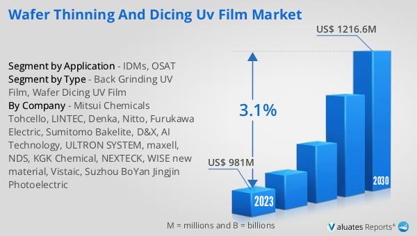
In the actual production process, this kind of film generally uses UV film. The global Wafer Thinning and Dicing UV Film market was valued at US$ 981 million in 2023 and is anticipated to reach US$ 1216.6 million by 2030, witnessing a CAGR of 3.1% during the forecast period 2024-2030. The largest region, Asia Pacific, declined by 2.0 percent. Sales in the Americas were US$142.1 billion, up 17.0% year-on-year; sales in Europe were US$53.8 billion, up 12.6% year-on-year; and sales in Japan were US$48.1 billion, up 10.0% year-on-year. However, sales in the largest Asia-Pacific region were US$336.2 billion, down 2.0% year-on-year.
| Report Metric | Details |
| Report Name | Wafer Thinning and Dicing UV Film Market |
| Accounted market size in 2023 | US$ 981 million |
| Forecasted market size in 2030 | US$ 1216.6 million |
| CAGR | 3.1% |
| Base Year | 2023 |
| Forecasted years | 2024 - 2030 |
| Segment by Type |
|
| Segment by Application |
|
| Production by Region |
|
| Consumption by Region |
|
| By Company | Mitsui Chemicals Tohcello, LINTEC, Denka, Nitto, Furukawa Electric, Sumitomo Bakelite, D&X, AI Technology, ULTRON SYSTEM, maxell, NDS, KGK Chemical, NEXTECK, WISE new material, Vistaic, Suzhou BoYan Jingjin Photoelectric |
| Forecast units | USD million in value |
| Report coverage | Revenue and volume forecast, company share, competitive landscape, growth factors and trends |


