Wednesday, March 5, 2025

Global LSI Test Probe Card Market Research Report 2025

What is Global LSI Test Probe Card Market?

The Global LSI Test Probe Card Market is an essential segment within the semiconductor industry, focusing on the tools used for testing integrated circuits (ICs) during the manufacturing process. These probe cards are critical for ensuring the functionality and reliability of semiconductor devices before they are packaged and shipped to customers. As the demand for more advanced and miniaturized electronic devices grows, the need for efficient and precise testing solutions becomes increasingly important. The market encompasses various types of probe cards, each designed to cater to specific testing requirements and technological advancements. With the rapid evolution of semiconductor technology, the Global LSI Test Probe Card Market is poised to play a crucial role in supporting the development and production of next-generation electronic devices. This market is driven by the continuous innovation in semiconductor manufacturing processes and the increasing complexity of IC designs, which necessitate more sophisticated testing solutions to maintain high quality and performance standards. As a result, the Global LSI Test Probe Card Market is expected to experience significant growth, driven by the ongoing advancements in semiconductor technology and the rising demand for high-performance electronic devices across various industries.

LSI Test Probe Card Market

Cantilever Probe Card, Vertical Probe Card, MEMS Probe Card, Others in the Global LSI Test Probe Card Market:

Cantilever Probe Cards are one of the most traditional types of probe cards used in the Global LSI Test Probe Card Market. These cards feature a simple design where the probes are arranged in a cantilever fashion, allowing them to make contact with the semiconductor wafer. Cantilever probe cards are known for their durability and cost-effectiveness, making them a popular choice for testing less complex ICs. However, as semiconductor technology advances, the limitations of cantilever probe cards, such as their inability to handle high pin counts and fine pitches, have become more apparent. This has led to the development of more advanced probe card technologies to meet the demands of modern semiconductor testing. Vertical Probe Cards, on the other hand, are designed to address some of the limitations of cantilever probe cards. These cards feature a vertical arrangement of probes, which allows for higher pin counts and finer pitches. Vertical probe cards are particularly well-suited for testing advanced ICs with complex designs and high-density interconnections. They offer improved performance and accuracy compared to cantilever probe cards, making them a preferred choice for testing cutting-edge semiconductor devices. The development of vertical probe cards has been driven by the need for more precise and efficient testing solutions in the semiconductor industry. MEMS (Micro-Electro-Mechanical Systems) Probe Cards represent a significant advancement in probe card technology. These cards utilize MEMS technology to create highly precise and reliable probes that can handle the demands of modern semiconductor testing. MEMS probe cards offer several advantages over traditional probe card designs, including higher accuracy, better repeatability, and the ability to test at higher frequencies. They are particularly well-suited for testing advanced semiconductor devices with complex architectures and high-performance requirements. The adoption of MEMS probe cards is expected to grow as the semiconductor industry continues to push the boundaries of technology and performance. In addition to these main types of probe cards, there are also other specialized probe card designs that cater to specific testing needs. These may include advanced probe cards with unique configurations or materials designed to address particular challenges in semiconductor testing. As the Global LSI Test Probe Card Market continues to evolve, the development of new and innovative probe card technologies will be essential to meet the ever-changing demands of the semiconductor industry. The ongoing advancements in probe card technology are expected to play a crucial role in supporting the growth and development of the semiconductor market, enabling the production of more advanced and reliable electronic devices.

Integrated Device Manufacturer (IDMs), Semiconductor Assembly and Test (OSAT) in the Global LSI Test Probe Card Market:

The Global LSI Test Probe Card Market plays a vital role in the operations of Integrated Device Manufacturers (IDMs) and Semiconductor Assembly and Test (OSAT) companies. IDMs are companies that design, manufacture, and sell integrated circuits, handling the entire semiconductor production process from start to finish. For IDMs, the use of probe cards is crucial in ensuring the quality and reliability of their semiconductor products. Probe cards are used during the wafer testing phase to verify the functionality of the ICs before they are packaged and shipped to customers. This testing process is essential for maintaining high quality standards and minimizing the risk of defects in the final products. As IDMs continue to develop more advanced and complex semiconductor devices, the demand for sophisticated probe card solutions is expected to grow. Semiconductor Assembly and Test (OSAT) companies, on the other hand, specialize in the assembly, packaging, and testing of semiconductor devices. These companies often work with multiple semiconductor manufacturers, providing them with the necessary testing and packaging services to ensure the quality and performance of their products. For OSAT companies, the use of probe cards is critical in the testing phase, where they verify the functionality and reliability of the semiconductor devices before they are packaged and delivered to customers. The Global LSI Test Probe Card Market provides OSAT companies with the advanced testing solutions they need to meet the demands of their clients and maintain high quality standards. As the semiconductor industry continues to evolve, the role of probe cards in the operations of IDMs and OSAT companies is becoming increasingly important. The ongoing advancements in probe card technology are enabling these companies to test more complex and advanced semiconductor devices with greater accuracy and efficiency. This is essential for maintaining the competitiveness of IDMs and OSAT companies in the rapidly changing semiconductor market. As a result, the Global LSI Test Probe Card Market is expected to experience significant growth, driven by the increasing demand for high-performance testing solutions in the semiconductor industry. The collaboration between probe card manufacturers, IDMs, and OSAT companies is crucial in driving innovation and ensuring the continued success of the semiconductor market.

Global LSI Test Probe Card Market Outlook:

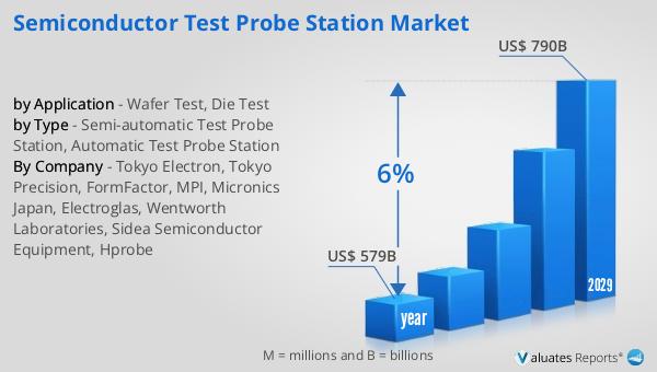
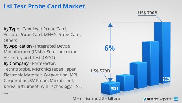
In 2022, the global semiconductor market was valued at approximately $579 billion. This figure is projected to rise significantly, reaching an estimated $790 billion by 2029. This growth trajectory represents a compound annual growth rate (CAGR) of 6% over the forecast period. The expansion of the semiconductor market is driven by several factors, including the increasing demand for advanced electronic devices, the proliferation of IoT (Internet of Things) applications, and the ongoing advancements in semiconductor technology. As the world becomes more interconnected and reliant on digital technologies, the demand for semiconductors is expected to continue its upward trend. The growth of the semiconductor market is also supported by the increasing adoption of artificial intelligence (AI), machine learning, and other emerging technologies that require high-performance semiconductor solutions. As a result, the Global LSI Test Probe Card Market is poised to benefit from this growth, as the demand for advanced testing solutions will rise in tandem with the expansion of the semiconductor market. The ongoing innovation in probe card technology will be essential in supporting the development and production of next-generation semiconductor devices, ensuring their quality and reliability in an increasingly competitive market.


Report Metric Details
Report Name LSI Test Probe Card Market
Accounted market size in year US$ 579 billion
Forecasted market size in 2029 US$ 790 billion
CAGR 6%
Base Year year
Forecasted years 2025 - 2029
by Type
  • Cantilever Probe Card
  • Vertical Probe Card
  • MEMS Probe Card
  • Others
by Application
  • Integrated Device Manufacturer (IDMs)
  • Semiconductor Assembly and Test (OSAT)
Production by Region
  • North America
  • Europe
  • China
  • Japan
  • South Korea
Consumption by Region
  • North America (United States, Canada)
  • Europe (Germany, France, UK, Italy, Russia)
  • Asia-Pacific (China, Japan, South Korea, Taiwan)
  • Southeast Asia (India)
  • Latin America (Mexico, Brazil)
By Company FormFactor, Technoprobe, Micronics Japan, Japan Electronic Materials Corporation, MPI Corporation, SV Probe, Microfriend, Korea Instrument, Will Technology, TSE, Feinmetall, Synergie Cad Probe, TIPS Messtechnik GmbH, STAr Technologies, Inc., MaxOne, Shenzhen DGT, Suzhou Silicon Test System, SPEA, Probecard Technology, Suzhou UIGreen Science and Technology, FastPrint, MMK
Forecast units USD million in value
Report coverage Revenue and volume forecast, company share, competitive landscape, growth factors and trends

Global Thick Film Current Sensing Resistor Market Research Report 2025

What is Global Thick Film Current Sensing Resistor Market?

The Global Thick Film Current Sensing Resistor Market is a specialized segment within the broader electronics industry, focusing on resistors that are essential for measuring electric current. These resistors are crafted using thick film technology, which involves applying a resistive film onto a ceramic substrate. This technology is favored for its cost-effectiveness and ability to handle high power levels, making it suitable for various applications. The market is driven by the increasing demand for efficient power management solutions across multiple sectors, including automotive, industrial, and consumer electronics. As industries continue to innovate and integrate more electronic components into their systems, the need for precise current measurement becomes crucial. This has led to a growing adoption of thick film current sensing resistors, which offer reliability and accuracy. The market is characterized by a diverse range of products, each tailored to meet specific requirements, such as resistance value, tolerance, and temperature coefficient. As technology advances, the market is expected to evolve, with manufacturers focusing on enhancing the performance and durability of these resistors to meet the ever-changing demands of modern electronic applications.

Thick Film Current Sensing Resistor Market

SMD, Through Hole in the Global Thick Film Current Sensing Resistor Market:

Surface-Mount Device (SMD) and Through-Hole technologies are two primary methods used in the assembly of electronic components, including those in the Global Thick Film Current Sensing Resistor Market. SMD technology involves mounting components directly onto the surface of printed circuit boards (PCBs). This method is highly favored in modern electronics due to its ability to support miniaturization and high-density circuit designs. SMD components, including thick film current sensing resistors, are typically smaller and lighter, which allows for more compact and efficient electronic devices. The use of SMD technology in thick film resistors is particularly advantageous in applications where space is limited, such as in smartphones, tablets, and other portable devices. Additionally, SMD components can be placed on both sides of a PCB, further optimizing space and design flexibility. On the other hand, Through-Hole technology involves inserting component leads through holes drilled into the PCB and soldering them in place. This method provides strong mechanical bonds, making it ideal for applications that require high reliability and durability, such as in automotive and industrial sectors. Through-Hole components are generally larger than their SMD counterparts, which can be beneficial in applications where component size is not a constraint. In the context of thick film current sensing resistors, Through-Hole technology is often used in environments that experience high levels of mechanical stress or where components need to withstand harsh conditions. The choice between SMD and Through-Hole technologies in the thick film current sensing resistor market largely depends on the specific requirements of the application, including factors such as size constraints, mechanical stress, and environmental conditions. Manufacturers in this market are continually innovating to improve the performance and reliability of both SMD and Through-Hole resistors, ensuring they meet the diverse needs of various industries. As electronic devices become more complex and demand for efficient power management solutions increases, the role of both SMD and Through-Hole technologies in the thick film current sensing resistor market is expected to remain significant. The ongoing advancements in these technologies are likely to drive further growth and innovation in the market, as manufacturers strive to develop resistors that offer enhanced performance, reliability, and cost-effectiveness.

Automotive, Industrial, Telecommunication, Consumer Electronic, Others in the Global Thick Film Current Sensing Resistor Market:

The Global Thick Film Current Sensing Resistor Market finds extensive usage across several key industries, including automotive, industrial, telecommunication, consumer electronics, and others. In the automotive sector, these resistors are crucial for managing and monitoring the electrical systems of vehicles. They are used in applications such as battery management systems, engine control units, and electric power steering, where precise current measurement is essential for optimal performance and safety. The demand for thick film current sensing resistors in the automotive industry is driven by the increasing adoption of electric and hybrid vehicles, which require efficient power management solutions. In the industrial sector, these resistors are used in various applications, including motor controls, power supplies, and energy management systems. They play a vital role in ensuring the efficient operation of industrial machinery and equipment by providing accurate current measurement and control. The telecommunication industry also relies on thick film current sensing resistors for managing power distribution and consumption in communication devices and infrastructure. These resistors help maintain the reliability and efficiency of telecommunication networks by ensuring stable power supply and preventing overloads. In the consumer electronics sector, thick film current sensing resistors are used in a wide range of devices, including smartphones, laptops, and home appliances. They enable efficient power management and contribute to the overall performance and longevity of electronic devices. Other industries, such as healthcare and aerospace, also utilize these resistors for various applications, highlighting their versatility and importance in modern technology. The widespread adoption of thick film current sensing resistors across these industries underscores their critical role in enabling efficient power management and enhancing the performance of electronic systems.

Global Thick Film Current Sensing Resistor Market Outlook:

In 2024, the global market for Thick Film Current Sensing Resistors was valued at approximately $1,646 million. Looking ahead, this market is anticipated to expand significantly, reaching an estimated value of $2,381 million by 2031. This growth trajectory represents a compound annual growth rate (CAGR) of 5.5% over the forecast period. The increasing demand for efficient power management solutions across various industries is a key driver of this market expansion. As electronic devices become more sophisticated and integrated into everyday life, the need for precise current measurement and control becomes increasingly important. Thick film current sensing resistors, known for their reliability and accuracy, are well-positioned to meet this demand. The market's growth is also supported by advancements in technology, which are enabling the development of resistors with enhanced performance and durability. As manufacturers continue to innovate and improve their products, the market is expected to evolve, offering new opportunities for growth and development. The projected increase in market size reflects the growing importance of thick film current sensing resistors in modern electronic applications and their critical role in enabling efficient power management.


Report Metric Details
Report Name Thick Film Current Sensing Resistor Market
Accounted market size in year US$ 1646 million
Forecasted market size in 2031 US$ 2381 million
CAGR 5.5%
Base Year year
Forecasted years 2025 - 2031
by Type
  • SMD
  • Through Hole
by Application
  • Automotive
  • Industrial
  • Telecommunication
  • Consumer Electronic
  • Others
Production by Region
  • North America
  • Europe
  • China
  • Japan
  • South Korea
Consumption by Region
  • North America (United States, Canada)
  • Europe (Germany, France, UK, Italy, Russia)
  • Asia-Pacific (China, Japan, South Korea, Taiwan)
  • Southeast Asia (India)
  • Latin America (Mexico, Brazil)
By Company Yageo, Isabellenhütte, TA-I Technology, KOA corporation, ROHM, Cyntec, Vishay, Panasonic, Walter, TT Electronics, Walsin Technology, Bourns, Viking Tech, TE Connectivity, Susumu, Ohmite, Samsung Electro-mechanics, Caddock
Forecast units USD million in value
Report coverage Revenue and volume forecast, company share, competitive landscape, growth factors and trends

Global FR4 Copper Clad Laminate Market Research Report 2025

What is Global FR4 Copper Clad Laminate Market?

The Global FR4 Copper Clad Laminate Market is a significant segment within the electronics industry, primarily due to its essential role in the manufacturing of printed circuit boards (PCBs). FR4 is a grade designation for flame-retardant fiberglass-reinforced epoxy laminate material. It is widely used because of its excellent mechanical strength, electrical insulation properties, and resistance to moisture. The copper-clad laminate is a crucial component in PCBs, serving as the substrate upon which electronic components are mounted. This market is driven by the increasing demand for electronic devices, advancements in technology, and the need for reliable and efficient electronic components. The growth of industries such as consumer electronics, telecommunications, and automotive electronics further fuels the demand for FR4 copper-clad laminates. As technology continues to evolve, the market is expected to adapt to new requirements, such as higher thermal performance and environmental sustainability. The global market for FR4 copper-clad laminates is characterized by a diverse range of products, catering to various applications and performance needs, making it a dynamic and vital part of the electronics manufacturing landscape.

FR4 Copper Clad Laminate Market

Low-end Sheet, Mid-end Sheet, High-end Sheet in the Global FR4 Copper Clad Laminate Market:

In the Global FR4 Copper Clad Laminate Market, products are typically categorized into low-end, mid-end, and high-end sheets, each serving different applications and performance requirements. Low-end sheets are generally used in applications where cost is a significant factor, and the performance requirements are not as stringent. These sheets are suitable for basic electronic devices and consumer products that do not require high thermal or electrical performance. They are often used in simple consumer electronics, toys, and other low-cost devices. The primary advantage of low-end sheets is their affordability, making them accessible for mass production of cost-sensitive products. Mid-end sheets, on the other hand, offer a balance between cost and performance. They are designed to meet moderate performance requirements and are commonly used in applications where reliability and durability are important but do not require the highest level of performance. These sheets are often found in more complex consumer electronics, communication devices, and industrial equipment. Mid-end sheets provide better thermal and electrical properties than low-end sheets, making them suitable for a wider range of applications. High-end sheets represent the top tier in the FR4 Copper Clad Laminate Market, offering superior performance characteristics. These sheets are engineered to meet the most demanding requirements in terms of thermal management, electrical insulation, and mechanical strength. High-end sheets are used in critical applications such as military and aerospace electronics, high-performance computing, and advanced communication systems. They are designed to withstand extreme conditions and provide reliable performance in challenging environments. The development of high-end sheets often involves advanced materials and manufacturing processes, resulting in higher costs compared to low-end and mid-end sheets. However, their superior performance justifies the investment for applications where failure is not an option. The choice between low-end, mid-end, and high-end sheets depends on the specific requirements of the application, including factors such as cost, performance, and environmental conditions. Manufacturers in the Global FR4 Copper Clad Laminate Market must carefully consider these factors to select the appropriate product for their needs. As technology continues to advance, the demand for higher performance materials is expected to grow, driving innovation and development in the market. This dynamic landscape requires manufacturers to continuously adapt and innovate to meet the evolving needs of their customers.

Military Industry, Consumer Electronics, Communication Network Equipment, Digital Circuits, Others in the Global FR4 Copper Clad Laminate Market:

The Global FR4 Copper Clad Laminate Market finds extensive usage across various industries, each with specific requirements and applications. In the military industry, FR4 copper-clad laminates are crucial for the production of reliable and durable electronic components used in defense equipment. These laminates must meet stringent standards for performance and reliability, as they are often used in critical applications such as radar systems, communication devices, and navigation equipment. The ability to withstand harsh environmental conditions and provide consistent performance is essential in military applications, making high-end FR4 laminates a preferred choice. In the consumer electronics sector, FR4 copper-clad laminates are widely used in the manufacturing of devices such as smartphones, tablets, and laptops. The demand for lightweight, compact, and high-performance electronic devices drives the need for efficient and reliable laminates. Mid-end and high-end sheets are commonly used in this sector to ensure the devices meet consumer expectations for performance and durability. The communication network equipment industry also relies heavily on FR4 copper-clad laminates for the production of routers, switches, and other networking devices. These laminates must provide excellent electrical insulation and thermal management to ensure the reliability and efficiency of communication systems. The growing demand for high-speed internet and advanced communication technologies further fuels the need for high-performance laminates in this sector. Digital circuits, which form the backbone of modern electronic devices, also utilize FR4 copper-clad laminates extensively. These laminates provide the necessary substrate for mounting and interconnecting electronic components, ensuring the circuits function correctly and efficiently. The choice of laminate in digital circuits depends on the specific performance requirements, with mid-end and high-end sheets often preferred for more complex and demanding applications. Beyond these specific industries, FR4 copper-clad laminates are used in a variety of other applications, including automotive electronics, industrial equipment, and medical devices. Each of these areas has unique requirements, driving the need for a diverse range of laminate products to meet specific performance and environmental conditions. The versatility and adaptability of FR4 copper-clad laminates make them an essential component in the global electronics industry, supporting a wide range of applications and technological advancements.

Global FR4 Copper Clad Laminate Market Outlook:

The outlook for the Global FR4 Copper Clad Laminate Market indicates a steady growth trajectory over the coming years. In 2024, the market was valued at approximately US$ 1,594 million, reflecting its significant role in the electronics manufacturing sector. By 2031, the market is expected to expand to a revised size of US$ 1,902 million, driven by a compound annual growth rate (CAGR) of 2.6% during the forecast period. This growth is attributed to the increasing demand for electronic devices across various industries, including consumer electronics, telecommunications, and automotive sectors. The need for reliable and efficient electronic components continues to rise as technology advances and new applications emerge. The market's expansion is also supported by ongoing innovations in materials and manufacturing processes, enabling the development of high-performance laminates that meet the evolving needs of the industry. As manufacturers strive to enhance the performance and sustainability of their products, the demand for advanced FR4 copper-clad laminates is expected to grow. This positive market outlook underscores the importance of FR4 copper-clad laminates in the global electronics landscape, highlighting their critical role in supporting technological progress and innovation.


Report Metric Details
Report Name FR4 Copper Clad Laminate Market
Accounted market size in year US$ 1594 million
Forecasted market size in 2031 US$ 1902 million
CAGR 2.6%
Base Year year
Forecasted years 2025 - 2031
by Type
  • Low-end Sheet
  • Mid-end Sheet
  • High-end Sheet
by Application
  • Military Industry
  • Consumer Electronics
  • Communication Network Equipment
  • Digital Circuits
  • Others
Production by Region
  • North America
  • Europe
  • China
  • Japan
  • South Korea
Consumption by Region
  • North America (United States, Canada)
  • Europe (Germany, France, UK, Italy, Russia)
  • Asia-Pacific (China, Japan, South Korea, Taiwan)
  • Southeast Asia (India)
  • Latin America (Mexico, Brazil)
By Company ROGERS, Mitsubishi Gas Chemical, Panasonic, Hitachi Chemical, Isola, ITEQ Corporation, TAIWAN POWDER TECHNOLOGIES, Nanya New Material Technology, Doosan Electronic, Kingboard Holdings Limited, Shengyi Technology, EMC, Nan Ya Plastics Corporation, Goldenmax International Technology, Zhejiang Wazam New Materials
Forecast units USD million in value
Report coverage Revenue and volume forecast, company share, competitive landscape, growth factors and trends

Global Quartz Chromium Photomask Market Research Report 2025

What is Global Quartz Chromium Photomask Market?

The Global Quartz Chromium Photomask Market is a specialized segment within the broader photomask industry, which plays a crucial role in the manufacturing of semiconductors and other electronic components. Photomasks are essential tools in the photolithography process, where they serve as templates for transferring intricate circuit patterns onto semiconductor wafers. Quartz chromium photomasks, in particular, are made from high-purity quartz glass and coated with a thin layer of chromium. This combination offers excellent optical properties and durability, making them ideal for high-precision applications. The market for these photomasks is driven by the increasing demand for advanced electronic devices, which require more complex and miniaturized components. As technology continues to evolve, the need for high-quality photomasks that can support the production of smaller and more efficient chips is expected to grow. This market is characterized by continuous innovation, as manufacturers strive to improve the resolution and accuracy of photomasks to meet the ever-increasing demands of the electronics industry. The global market for quartz chromium photomasks is poised for steady growth, driven by advancements in semiconductor technology and the expanding applications of electronic devices across various industries.

Quartz Chromium Photomask Market

Synthetic Chromium Masks, Ordinary Chromium Masks in the Global Quartz Chromium Photomask Market:

Synthetic Chromium Masks and Ordinary Chromium Masks are two distinct types of photomasks used in the Global Quartz Chromium Photomask Market, each serving specific purposes and offering unique advantages. Synthetic Chromium Masks are designed for high-precision applications where accuracy and resolution are paramount. These masks are typically used in the production of advanced semiconductor devices, where even the slightest deviation in pattern transfer can lead to significant performance issues. The synthetic chromium layer on these masks is engineered to provide superior optical clarity and minimal defects, ensuring that the intricate patterns required for modern electronic components are accurately reproduced. This makes them ideal for cutting-edge technologies such as microprocessors and memory chips, where the demand for smaller and more efficient components is ever-increasing. On the other hand, Ordinary Chromium Masks are more commonly used for less demanding applications where the requirements for precision and resolution are not as stringent. These masks are often employed in the production of larger electronic components or in industries where cost-effectiveness is a primary concern. While they may not offer the same level of precision as their synthetic counterparts, ordinary chromium masks are still highly effective for a wide range of applications. They provide a reliable and economical solution for manufacturers looking to produce electronic components at scale without compromising on quality. The choice between synthetic and ordinary chromium masks often depends on the specific requirements of the application, with factors such as cost, precision, and production volume playing a crucial role in the decision-making process. As the demand for electronic devices continues to grow, both types of masks are expected to play a vital role in supporting the diverse needs of the electronics industry. Manufacturers are continually investing in research and development to enhance the performance and capabilities of these masks, ensuring that they can meet the evolving demands of the market. This ongoing innovation is essential for maintaining the competitiveness of the Global Quartz Chromium Photomask Market and supporting the advancement of semiconductor technology. As technology continues to advance, the distinction between synthetic and ordinary chromium masks may become more pronounced, with each type catering to increasingly specialized applications. This specialization is likely to drive further growth and diversification within the market, as manufacturers seek to capitalize on the unique strengths of each type of mask. Ultimately, the success of the Global Quartz Chromium Photomask Market will depend on its ability to adapt to the changing needs of the electronics industry and continue providing high-quality solutions that enable the production of next-generation electronic devices.

Semiconductor, Flat Panel Display, Touch Industry, Circuit Board in the Global Quartz Chromium Photomask Market:

The Global Quartz Chromium Photomask Market finds extensive usage across several key industries, including semiconductors, flat panel displays, the touch industry, and circuit boards. In the semiconductor industry, photomasks are indispensable tools used in the photolithography process to create intricate patterns on silicon wafers. These patterns form the basis of integrated circuits, which are the building blocks of all electronic devices. As the demand for smaller, faster, and more efficient chips continues to grow, the need for high-precision photomasks becomes increasingly critical. Quartz chromium photomasks, with their superior optical properties and durability, are ideally suited to meet these demands, enabling the production of advanced semiconductor devices that power everything from smartphones to supercomputers. In the flat panel display industry, photomasks are used to create the intricate patterns required for the production of liquid crystal displays (LCDs) and organic light-emitting diode (OLED) screens. These displays are ubiquitous in modern consumer electronics, including televisions, monitors, and mobile devices. The precision and accuracy of quartz chromium photomasks ensure that the displays produced are of the highest quality, with vibrant colors and sharp images. As the demand for high-resolution displays continues to rise, the role of photomasks in this industry becomes even more crucial. The touch industry, which encompasses touchscreens and touch-sensitive devices, also relies heavily on photomasks for the production of touch sensors. These sensors are integral components of modern user interfaces, enabling intuitive and responsive interactions with electronic devices. Quartz chromium photomasks are used to create the fine patterns required for these sensors, ensuring that they function accurately and reliably. As touch technology becomes increasingly prevalent in a wide range of applications, from smartphones to automotive displays, the demand for high-quality photomasks in this industry is expected to grow. Finally, in the circuit board industry, photomasks are used to transfer circuit patterns onto printed circuit boards (PCBs), which are essential components of virtually all electronic devices. The precision and accuracy of quartz chromium photomasks ensure that the circuit patterns are transferred accurately, minimizing defects and ensuring the reliability of the final product. As electronic devices become more complex and compact, the need for high-quality photomasks in the circuit board industry becomes increasingly important. Overall, the Global Quartz Chromium Photomask Market plays a vital role in supporting the production of a wide range of electronic devices across multiple industries. The ongoing demand for smaller, faster, and more efficient electronic components drives the need for high-precision photomasks, ensuring that this market remains a critical component of the global electronics supply chain.

Global Quartz Chromium Photomask Market Outlook:

In 2024, the worldwide market for Quartz Chromium Photomask was estimated to be worth approximately $5,791 million. Looking ahead, this market is anticipated to expand, reaching an adjusted valuation of around $7,967 million by the year 2031. This growth trajectory represents a compound annual growth rate (CAGR) of 4.7% over the forecast period. This steady increase underscores the rising demand for quartz chromium photomasks, driven by advancements in technology and the growing need for high-precision electronic components. As industries such as semiconductors, flat panel displays, and touch technology continue to evolve, the demand for high-quality photomasks is expected to rise correspondingly. The projected growth in the market reflects the critical role that quartz chromium photomasks play in the production of advanced electronic devices. Manufacturers are likely to continue investing in research and development to enhance the capabilities of these photomasks, ensuring that they can meet the ever-increasing demands of the electronics industry. This ongoing innovation is essential for maintaining the competitiveness of the Global Quartz Chromium Photomask Market and supporting the advancement of semiconductor technology. As the market continues to grow, it will be important for stakeholders to stay abreast of the latest developments and trends to capitalize on the opportunities presented by this dynamic and rapidly evolving industry.


Report Metric Details
Report Name Quartz Chromium Photomask Market
Accounted market size in year US$ 5791 million
Forecasted market size in 2031 US$ 7967 million
CAGR 4.7%
Base Year year
Forecasted years 2025 - 2031
by Type
  • Synthetic Chromium Masks
  • Ordinary Chromium Masks
by Application
  • Semiconductor
  • Flat Panel Display
  • Touch Industry
  • Circuit Board
Production by Region
  • North America
  • Europe
  • China
  • Japan
  • South Korea
Consumption by Region
  • North America (United States, Canada)
  • Europe (Germany, France, UK, Italy, Russia)
  • Asia-Pacific (China, Japan, South Korea, Taiwan)
  • Southeast Asia (India)
  • Latin America (Mexico, Brazil)
By Company Photronics, Toppan, DNP, Hoya, SK-Electronics, LG Innotek, ShenZheng QingVi, Taiwan Mask, Nippon Filcon, Compugraphics, Newway Photomask
Forecast units USD million in value
Report coverage Revenue and volume forecast, company share, competitive landscape, growth factors and trends

Global Dual-technology Occupancy Sensors Market Research Report 2025

What is Global Dual-technology Occupancy Sensors Market?

The Global Dual-technology Occupancy Sensors Market is an evolving segment within the broader field of smart building technologies. These sensors are designed to enhance energy efficiency and optimize space utilization by detecting human presence in a room or area. They employ a combination of two technologies, typically passive infrared (PIR) and ultrasonic, to accurately sense occupancy. PIR sensors detect motion based on heat emitted by the human body, while ultrasonic sensors use sound waves to detect movement. This dual approach minimizes false readings and ensures reliable performance in various environments. The market for these sensors is driven by the increasing demand for energy-efficient solutions in commercial and residential buildings. As businesses and homeowners seek to reduce energy consumption and costs, dual-technology occupancy sensors offer a practical solution by automatically controlling lighting, heating, and cooling systems based on real-time occupancy data. Additionally, the growing trend of smart homes and buildings, coupled with stringent government regulations on energy efficiency, further propels the market's growth. As a result, manufacturers are continuously innovating to develop more advanced sensors that offer improved accuracy, ease of installation, and integration with other smart systems.

Dual-technology Occupancy Sensors Market

Wall Mounted, Ceiling Mounted, Others in the Global Dual-technology Occupancy Sensors Market:

In the Global Dual-technology Occupancy Sensors Market, the types of sensors available include wall-mounted, ceiling-mounted, and other configurations, each serving distinct purposes and offering unique advantages. Wall-mounted sensors are typically installed at a height where they can effectively cover a wide area. They are ideal for spaces where the sensor needs to detect motion across a horizontal plane, such as hallways, corridors, and open office spaces. These sensors are often preferred for their ease of installation and maintenance, as they can be easily accessed for adjustments or repairs. Wall-mounted sensors are designed to blend seamlessly with the interior decor, ensuring that they do not detract from the aesthetic appeal of the space. Ceiling-mounted sensors, on the other hand, are installed on the ceiling and are particularly effective in spaces where a 360-degree coverage is required. They are commonly used in rooms with high ceilings or where there is a need to detect occupancy across a large area, such as conference rooms, auditoriums, and large open-plan offices. Ceiling-mounted sensors offer the advantage of being less obtrusive, as they are positioned out of the line of sight, and they can cover a larger area with fewer units compared to wall-mounted sensors. This makes them a cost-effective solution for large spaces. Other configurations of dual-technology occupancy sensors include corner-mounted and portable sensors. Corner-mounted sensors are designed to be installed in the corners of a room, providing coverage for areas that might be missed by wall or ceiling-mounted sensors. They are particularly useful in irregularly shaped rooms or spaces with obstacles that could block the sensor's line of sight. Portable sensors, meanwhile, offer flexibility and convenience, as they can be moved and repositioned as needed. These sensors are ideal for temporary installations or spaces where the layout frequently changes, such as exhibition halls or event venues. The choice between wall-mounted, ceiling-mounted, and other configurations depends on various factors, including the size and layout of the space, the desired coverage area, and the specific requirements of the application. For instance, in a small office, a wall-mounted sensor might suffice, while a large conference room might benefit from the comprehensive coverage offered by a ceiling-mounted sensor. Additionally, the type of sensor chosen can impact the overall energy efficiency and effectiveness of the occupancy detection system. By selecting the appropriate sensor configuration, businesses and homeowners can ensure optimal performance and maximize the benefits of their dual-technology occupancy sensors.

Meeting Room, Classroom, Large Office, Others in the Global Dual-technology Occupancy Sensors Market:

The Global Dual-technology Occupancy Sensors Market finds extensive application in various settings, including meeting rooms, classrooms, large offices, and other areas. In meeting rooms, these sensors play a crucial role in enhancing energy efficiency and ensuring a comfortable environment for attendees. By detecting when a room is occupied, the sensors can automatically adjust lighting and climate control systems, reducing energy consumption when the room is empty. This not only helps in cutting down on energy costs but also contributes to a more sustainable and environmentally friendly operation. In classrooms, dual-technology occupancy sensors are used to create an optimal learning environment. They ensure that lights and HVAC systems are only active when the room is in use, preventing unnecessary energy wastage. This is particularly important in educational institutions where multiple classrooms are in use simultaneously, and energy efficiency can lead to significant cost savings. Moreover, these sensors help maintain a comfortable temperature and lighting level, which can enhance students' concentration and learning experience. In large offices, occupancy sensors are essential for managing energy use across vast spaces with numerous workstations. They enable facilities managers to monitor and control lighting and climate systems based on real-time occupancy data, ensuring that energy is not wasted in unoccupied areas. This is especially beneficial in open-plan offices where different sections may be in use at different times. By optimizing energy use, businesses can reduce their operational costs and improve their sustainability credentials. Beyond these specific areas, dual-technology occupancy sensors are also used in various other settings, such as restrooms, corridors, and storage rooms. In restrooms, they ensure that lights are only on when the facilities are in use, enhancing energy efficiency and reducing electricity bills. In corridors and hallways, these sensors help maintain safety and security by ensuring that lights are always on when people are present, while also conserving energy when the area is empty. In storage rooms and other less frequently used spaces, occupancy sensors prevent lights from being left on unnecessarily, contributing to overall energy savings. The versatility and adaptability of dual-technology occupancy sensors make them a valuable addition to any building, helping to create smarter, more efficient, and more sustainable environments.

Global Dual-technology Occupancy Sensors Market Outlook:

The worldwide semiconductor market, valued at approximately $579 billion in 2022, is anticipated to reach around $790 billion by 2029, reflecting a compound annual growth rate (CAGR) of 6% over the forecast period. This growth trajectory underscores the increasing demand for semiconductors across various industries, driven by advancements in technology and the proliferation of electronic devices. Semiconductors are integral components in a wide range of applications, from consumer electronics and automotive systems to industrial machinery and telecommunications. The rising adoption of technologies such as artificial intelligence, the Internet of Things (IoT), and 5G connectivity is further fueling the demand for semiconductors, as these technologies require advanced processing capabilities and efficient power management. Additionally, the ongoing digital transformation across industries is contributing to the expansion of the semiconductor market, as businesses seek to leverage data-driven insights and automation to enhance their operations. As the market continues to grow, manufacturers are investing in research and development to innovate and produce more efficient and powerful semiconductor solutions. This includes the development of smaller, faster, and more energy-efficient chips that can meet the evolving needs of modern applications. The projected growth of the semiconductor market highlights the critical role these components play in enabling technological progress and shaping the future of various industries.


Report Metric Details
Report Name Dual-technology Occupancy Sensors Market
Accounted market size in year US$ 579 billion
Forecasted market size in 2029 US$ 790 billion
CAGR 6%
Base Year year
Forecasted years 2025 - 2029
by Type
  • Wall Mounted
  • Ceiling Mounted
  • Others
by Application
  • Meeting Room
  • Classroom
  • Large Office
  • Others
Production by Region
  • North America
  • Europe
  • China
  • Japan
  • South Korea
Consumption by Region
  • North America (United States, Canada)
  • Europe (Germany, France, UK, Italy, Russia)
  • Asia-Pacific (China, Japan, South Korea, Taiwan)
  • Southeast Asia (India)
  • Latin America (Mexico, Brazil)
By Company Legrand, Signify, Crestron Electronics, Schneider Electric, Honeywell, Johnson Controls, Acuity Brands, GE Current, SENSOR WORX, Leviton Manufacturing, OPTEX, Lutron Electronics, Enerlites
Forecast units USD million in value
Report coverage Revenue and volume forecast, company share, competitive landscape, growth factors and trends

Global TZP Ceramics Beads Market Research Report 2025

What is Global TZP Ceramics Beads Market?

The Global TZP Ceramics Beads Market is a specialized segment within the broader ceramics industry, focusing on the production and application of tetragonal zirconia polycrystal (TZP) beads. These beads are renowned for their exceptional mechanical properties, including high fracture toughness, wear resistance, and thermal stability, making them ideal for various industrial applications. TZP ceramics beads are primarily composed of zirconium dioxide (ZrO2) and are stabilized in the tetragonal phase, which enhances their durability and performance under stress. The market for these beads is driven by their increasing use in industries such as electronics, pharmaceuticals, and manufacturing, where precision and reliability are paramount. As industries continue to demand materials that can withstand harsh conditions and deliver consistent performance, the TZP ceramics beads market is poised for growth. The global market dynamics are influenced by technological advancements, research and development activities, and the growing need for high-performance materials in emerging economies. With a focus on innovation and sustainability, manufacturers are exploring new applications and improving production techniques to meet the evolving needs of various sectors.

TZP Ceramics Beads Market

Y-TZP Bead, Ce-TZP Bead, Others in the Global TZP Ceramics Beads Market:

Y-TZP beads, Ce-TZP beads, and other variants play a crucial role in the Global TZP Ceramics Beads Market, each offering unique properties that cater to specific industrial needs. Y-TZP beads, or yttria-stabilized tetragonal zirconia polycrystal beads, are the most common type, known for their superior mechanical strength and resistance to wear and corrosion. These beads are stabilized with yttria (Y2O3), which helps maintain the tetragonal phase at room temperature, ensuring high durability and fracture toughness. Y-TZP beads are widely used in applications requiring high precision and reliability, such as in the electronics and automotive industries, where they contribute to the longevity and efficiency of components. Ce-TZP beads, on the other hand, are stabilized with ceria (CeO2) and are valued for their excellent thermal stability and resistance to thermal shock. These beads are particularly useful in high-temperature applications, where maintaining structural integrity is crucial. The addition of ceria enhances the beads' ability to withstand rapid temperature changes without compromising their mechanical properties. Ce-TZP beads find applications in industries such as aerospace and energy, where materials are subjected to extreme conditions and require exceptional performance. Apart from Y-TZP and Ce-TZP beads, the market also includes other variants that are tailored to meet specific industrial requirements. These may include beads stabilized with different oxides or those with modified compositions to enhance certain properties. For instance, some beads may be engineered to offer improved electrical conductivity or magnetic properties, expanding their use in specialized applications. The diversity of TZP ceramics beads allows manufacturers to cater to a wide range of industries, each with its unique set of challenges and demands. The production of TZP ceramics beads involves advanced manufacturing techniques to ensure uniformity and consistency in size and shape, which are critical for their performance. Precision in manufacturing is essential to achieve the desired mechanical and thermal properties, making the production process a key focus area for manufacturers. Continuous research and development efforts are directed towards optimizing production methods, reducing costs, and enhancing the properties of TZP beads to meet the evolving needs of various industries. In summary, Y-TZP beads, Ce-TZP beads, and other variants form the backbone of the Global TZP Ceramics Beads Market, each offering distinct advantages that cater to specific industrial applications. The choice of bead type depends on the specific requirements of the application, such as mechanical strength, thermal stability, or resistance to wear and corrosion. As industries continue to seek high-performance materials that can withstand demanding conditions, the demand for TZP ceramics beads is expected to grow, driven by innovation and advancements in manufacturing technologies.

Electronic Industry, Paper/Paint/Ink, Food/Pharmaceutical/Cosmetics, Others in the Global TZP Ceramics Beads Market:

The Global TZP Ceramics Beads Market finds extensive usage across various industries, each leveraging the unique properties of these beads to enhance their processes and products. In the electronic industry, TZP ceramics beads are used in the manufacturing of components that require high precision and reliability. Their excellent mechanical strength and resistance to wear make them ideal for use in electronic devices, where they contribute to the durability and performance of components such as capacitors, resistors, and connectors. The ability of TZP beads to withstand high temperatures and harsh environments ensures the longevity and efficiency of electronic devices, making them a preferred choice for manufacturers seeking to improve product quality and performance. In the paper, paint, and ink industries, TZP ceramics beads are used as grinding media in the milling process. Their high density and hardness make them effective in reducing particle size and achieving a uniform dispersion of pigments and other materials. This results in improved product quality, with enhanced color strength and consistency in paints and inks. The use of TZP beads in these industries also contributes to increased efficiency and reduced production costs, as they offer longer service life and require less frequent replacement compared to other grinding media. The food, pharmaceutical, and cosmetics industries also benefit from the use of TZP ceramics beads, particularly in processes that require high purity and contamination-free environments. In the pharmaceutical industry, TZP beads are used in the production of active pharmaceutical ingredients (APIs) and other formulations, where their inert nature and resistance to chemical reactions ensure product safety and efficacy. Similarly, in the food and cosmetics industries, TZP beads are used in processes such as homogenization and emulsification, where maintaining product integrity and quality is crucial. The use of TZP beads in these industries helps manufacturers achieve consistent product quality while adhering to stringent regulatory standards. Beyond these industries, TZP ceramics beads are also used in other applications, such as in the production of advanced ceramics and composites, where their unique properties contribute to the development of high-performance materials. The versatility of TZP beads allows them to be used in a wide range of applications, from automotive components to medical devices, where their mechanical and thermal properties are leveraged to enhance product performance and reliability. In conclusion, the Global TZP Ceramics Beads Market plays a vital role in various industries, each benefiting from the unique properties of these beads to improve their processes and products. The demand for TZP beads is driven by the need for high-performance materials that can withstand demanding conditions and deliver consistent results. As industries continue to evolve and seek innovative solutions, the use of TZP ceramics beads is expected to grow, supported by advancements in manufacturing technologies and a focus on sustainability and efficiency.

Global TZP Ceramics Beads Market Outlook:

In 2024, the global market for TZP Ceramics Beads was estimated to be worth approximately $587 million. Looking ahead, projections indicate that by 2031, this market is expected to expand significantly, reaching an estimated value of $929 million. This growth trajectory reflects a compound annual growth rate (CAGR) of 6.8% over the forecast period. This upward trend underscores the increasing demand for TZP ceramics beads across various industries, driven by their superior mechanical properties and versatility in applications ranging from electronics to pharmaceuticals. The market's expansion is also indicative of the ongoing advancements in manufacturing technologies and the continuous pursuit of high-performance materials that meet the evolving needs of modern industries. As the market grows, manufacturers are likely to focus on innovation and sustainability, exploring new applications and improving production techniques to maintain a competitive edge. The projected growth of the TZP ceramics beads market highlights the importance of these materials in addressing the challenges faced by industries seeking reliable and efficient solutions. With a focus on quality and performance, the market is poised to play a crucial role in the development of advanced materials and technologies in the coming years.


Report Metric Details
Report Name TZP Ceramics Beads Market
Accounted market size in year US$ 587 million
Forecasted market size in 2031 US$ 929 million
CAGR 6.8%
Base Year year
Forecasted years 2025 - 2031
by Type
  • Y-TZP Bead
  • Ce-TZP Bead
  • Others
by Application
  • Electronic Industry
  • Paper/Paint/Ink
  • Food/Pharmaceutical/Cosmetics
  • Others
Production by Region
  • North America
  • Europe
  • China
  • Japan
Consumption by Region
  • North America (United States, Canada)
  • Europe (Germany, France, UK, Italy, Russia)
  • Asia-Pacific (China, Japan, South Korea, Taiwan)
  • Southeast Asia (India)
  • Latin America (Mexico, Brazil)
By Company Saint-Gobain ZirPro, Tosoh, Dynamech, Toray, CENOTEC, Orient Zirconic, Shandong Hanhe New Materials, CHEMCO, Zhejiang Humo Polishing Grinder Manufacture, Ganzhou Koin Structure Ceramics, Sigmund Lindner GmbH
Forecast units USD million in value
Report coverage Revenue and volume forecast, company share, competitive landscape, growth factors and trends

Global Semiconductor Test Probe Station Market Research Report 2025

What is Global Semiconductor Test Probe Station Market?

The Global Semiconductor Test Probe Station Market is a crucial segment within the semiconductor industry, focusing on the equipment used to test semiconductor wafers and dies. These test probe stations are essential for ensuring the quality and functionality of semiconductor devices before they are packaged and shipped to customers. The market encompasses a variety of probe stations, each designed to meet specific testing needs, ranging from manual to fully automated systems. These stations are used to test electrical parameters, identify defects, and ensure that the semiconductor devices meet the required specifications. The demand for semiconductor test probe stations is driven by the increasing complexity of semiconductor devices, the need for higher performance, and the rapid pace of technological advancements. As the semiconductor industry continues to grow, driven by the proliferation of electronic devices, the Internet of Things (IoT), and advancements in artificial intelligence and machine learning, the demand for efficient and accurate testing solutions is expected to rise. This market is characterized by continuous innovation, with manufacturers focusing on developing advanced probe stations that offer higher precision, faster testing speeds, and greater automation to meet the evolving needs of the semiconductor industry.

Semiconductor Test Probe Station Market

Semi-automatic Test Probe Station, Automatic Test Probe Station in the Global Semiconductor Test Probe Station Market:

In the Global Semiconductor Test Probe Station Market, semi-automatic and automatic test probe stations play a pivotal role in the testing process of semiconductor devices. Semi-automatic test probe stations are designed to offer a balance between manual intervention and automation. These stations typically require an operator to load and unload wafers or dies, but the testing process itself is automated. This type of station is ideal for environments where flexibility is needed, as they allow for quick adjustments and are suitable for testing a wide range of semiconductor devices. Semi-automatic stations are often used in research and development settings or in production environments where the volume of testing is moderate. They provide a cost-effective solution for companies that need a certain level of automation without the high investment required for fully automated systems. On the other hand, automatic test probe stations are designed for high-volume production environments where speed and efficiency are paramount. These stations are fully automated, meaning that they can handle the entire testing process from loading to unloading without human intervention. Automatic test probe stations are equipped with advanced robotics and software that allow for precise and rapid testing of semiconductor devices. They are ideal for large-scale manufacturing operations where consistency and throughput are critical. The use of automatic test probe stations can significantly reduce the time and labor costs associated with the testing process, making them a valuable investment for companies looking to optimize their production lines. Both semi-automatic and automatic test probe stations are integral to the semiconductor manufacturing process, ensuring that devices meet the stringent quality standards required by the industry. As the demand for semiconductors continues to grow, driven by advancements in technology and the increasing complexity of electronic devices, the need for efficient and reliable testing solutions will remain a key focus for manufacturers in the Global Semiconductor Test Probe Station Market.

Wafer Test, Die Test in the Global Semiconductor Test Probe Station Market:

The Global Semiconductor Test Probe Station Market finds significant application in wafer testing and die testing, two critical stages in the semiconductor manufacturing process. Wafer testing, also known as wafer probing, involves testing the semiconductor wafers before they are diced into individual dies. This stage is crucial for identifying any defects or issues in the wafer that could affect the performance of the final semiconductor devices. Test probe stations used in wafer testing are equipped with precision probes that make contact with the wafer's test pads to measure electrical parameters and ensure that the wafer meets the required specifications. This process helps in identifying defective wafers early in the production process, reducing waste and improving overall yield. Die testing, on the other hand, occurs after the wafer has been diced into individual semiconductor dies. This stage involves testing each die to ensure that it functions correctly before it is packaged and shipped to customers. Test probe stations used in die testing are designed to handle small, delicate dies and are equipped with advanced probing technology to ensure accurate and reliable testing. Die testing is essential for ensuring the quality and reliability of semiconductor devices, as any defects at this stage can lead to failures in the final product. The use of test probe stations in both wafer and die testing is critical for maintaining the high quality standards required in the semiconductor industry. As semiconductor devices become more complex and the demand for higher performance increases, the need for precise and efficient testing solutions will continue to grow. The Global Semiconductor Test Probe Station Market is poised to play a key role in meeting these demands, providing manufacturers with the tools they need to ensure the quality and reliability of their products.

Global Semiconductor Test Probe Station Market Outlook:

The global semiconductor market was valued at approximately $579 billion in 2022, and it is anticipated to reach around $790 billion by 2029, reflecting a compound annual growth rate (CAGR) of 6% over the forecast period. This growth is indicative of the increasing demand for semiconductors across various industries, driven by technological advancements and the proliferation of electronic devices. The semiconductor industry is a cornerstone of modern technology, providing the essential components that power everything from smartphones and computers to advanced medical devices and automotive systems. As the world becomes increasingly digital, the demand for semiconductors is expected to continue its upward trajectory. The projected growth in the semiconductor market underscores the importance of efficient and reliable testing solutions, such as those provided by the Global Semiconductor Test Probe Station Market. These testing solutions are critical for ensuring the quality and performance of semiconductor devices, which in turn supports the overall growth and innovation within the industry. As manufacturers strive to meet the evolving needs of their customers, the role of test probe stations in the semiconductor manufacturing process will remain vital, ensuring that devices meet the stringent quality standards required in today's competitive market.


Report Metric Details
Report Name Semiconductor Test Probe Station Market
Accounted market size in year US$ 579 billion
Forecasted market size in 2029 US$ 790 billion
CAGR 6%
Base Year year
Forecasted years 2025 - 2029
by Type
  • Semi-automatic Test Probe Station
  • Automatic Test Probe Station
by Application
  • Wafer Test
  • Die Test
Production by Region
  • North America
  • Europe
  • China
  • Japan
Consumption by Region
  • North America (United States, Canada)
  • Europe (Germany, France, UK, Italy, Russia)
  • Asia-Pacific (China, Japan, South Korea, Taiwan)
  • Southeast Asia (India)
  • Latin America (Mexico, Brazil)
By Company Tokyo Electron, Tokyo Precision, FormFactor, MPI, Micronics Japan, Electroglas, Wentworth Laboratories, Sidea Semiconductor Equipment, Hprobe
Forecast units USD million in value
Report coverage Revenue and volume forecast, company share, competitive landscape, growth factors and trends

Global Military Radiation Detector Market Research Report 2025

What is Global Military Radiation Detector Market? The Global Military Radiation Detector Market is a specialized segment within the broade...