What is Global Semiconductor Processing Equipment Market?
The Global Semiconductor Processing Equipment Market is a crucial segment of the broader semiconductor industry, which is integral to the production of electronic devices. This market encompasses a wide range of equipment used in the manufacturing of semiconductors, which are essential components in electronic devices like smartphones, computers, and various digital appliances. The equipment includes tools for processes such as lithography, etching, deposition, and cleaning, each playing a vital role in the creation of semiconductor wafers. As technology advances, the demand for more sophisticated and efficient semiconductor processing equipment grows, driven by the need for smaller, faster, and more energy-efficient electronic devices. The market is influenced by factors such as technological advancements, the rise of the Internet of Things (IoT), and the increasing demand for consumer electronics. Companies in this market are continually innovating to improve the precision and efficiency of their equipment, ensuring they meet the evolving needs of semiconductor manufacturers. The global reach of this market is significant, with major players operating in regions like North America, Europe, and Asia, each contributing to the development and distribution of cutting-edge semiconductor processing technologies.
Lithography, Wafer Surface Conditioning, Cleaning Processes in the Global Semiconductor Processing Equipment Market:
Lithography, wafer surface conditioning, and cleaning processes are fundamental components of the Global Semiconductor Processing Equipment Market, each playing a critical role in the production of semiconductor devices. Lithography is a process used to transfer a pattern from a photomask to the surface of a semiconductor wafer. This is achieved by coating the wafer with a light-sensitive material called photoresist, which is then exposed to light through the photomask. The exposed areas of the photoresist are then developed, leaving a pattern that can be etched into the wafer. This process is crucial for defining the intricate circuits that make up semiconductor devices. Advances in lithography, such as extreme ultraviolet (EUV) lithography, have enabled the production of smaller and more complex semiconductor devices, meeting the demand for high-performance electronics. Wafer surface conditioning involves preparing the surface of the wafer for subsequent processing steps. This includes processes such as planarization, which ensures a flat and smooth surface, and doping, which introduces impurities into the wafer to modify its electrical properties. These steps are essential for ensuring the quality and performance of the final semiconductor device. Cleaning processes are also vital in semiconductor manufacturing, as even the smallest particles or contaminants can affect the performance of the final product. Cleaning involves removing any unwanted materials from the wafer surface, using techniques such as wet cleaning, dry cleaning, and chemical mechanical polishing (CMP). Each of these processes must be carefully controlled to ensure the integrity of the wafer and the success of subsequent processing steps. The equipment used in these processes is continually evolving, with manufacturers developing new technologies to improve efficiency, precision, and yield. As the demand for smaller, faster, and more energy-efficient semiconductor devices grows, the importance of advanced lithography, wafer surface conditioning, and cleaning processes in the Global Semiconductor Processing Equipment Market cannot be overstated. These processes are at the heart of semiconductor manufacturing, enabling the production of the high-performance electronic devices that are essential to modern life.
Assembly & Packaging, Dicing, Bonding, Metrology in the Global Semiconductor Processing Equipment Market:
The Global Semiconductor Processing Equipment Market plays a significant role in various stages of semiconductor manufacturing, including assembly and packaging, dicing, bonding, and metrology. Assembly and packaging involve enclosing the semiconductor die in a protective package that allows it to be connected to external circuits. This process is crucial for protecting the delicate semiconductor components from physical damage and environmental factors. Advanced packaging technologies, such as 3D packaging and system-in-package (SiP), are becoming increasingly important as they allow for higher performance and greater functionality in a smaller form factor. Dicing is the process of cutting the semiconductor wafer into individual dies, which are then used to create semiconductor devices. This process requires precision equipment to ensure clean and accurate cuts, minimizing damage to the delicate semiconductor material. Bonding involves attaching the semiconductor die to a substrate or package, using techniques such as wire bonding or flip-chip bonding. This step is critical for ensuring a reliable electrical connection between the die and the external circuitry. Metrology, on the other hand, involves measuring and analyzing the physical and electrical properties of the semiconductor devices to ensure they meet the required specifications. This includes inspecting the dimensions of the features on the wafer, as well as testing the electrical performance of the devices. Advanced metrology equipment is essential for maintaining the quality and reliability of semiconductor products, as it allows manufacturers to detect and correct any defects or variations in the manufacturing process. The Global Semiconductor Processing Equipment Market is continually evolving, with manufacturers developing new technologies to improve the efficiency and precision of these processes. As the demand for smaller, faster, and more energy-efficient semiconductor devices grows, the importance of advanced assembly and packaging, dicing, bonding, and metrology equipment cannot be overstated. These processes are essential for ensuring the quality and performance of the final semiconductor products, enabling the production of the high-performance electronic devices that are essential to modern life.
Global Semiconductor Processing Equipment Market Outlook:
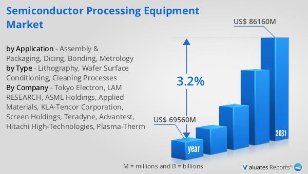
In 2024, the global market for Semiconductor Processing Equipment was valued at approximately $69.56 billion. This market is anticipated to expand, reaching an estimated size of $86.16 billion by 2031, reflecting a compound annual growth rate (CAGR) of 3.2% over the forecast period. This growth is indicative of the increasing demand for advanced semiconductor processing technologies, driven by the rapid evolution of electronic devices and the need for more efficient and powerful semiconductors. The market's expansion is supported by technological advancements and the rising adoption of semiconductors in various applications, including consumer electronics, automotive, and industrial sectors. Notably, regions such as North America, Europe, and Japan collectively hold a significant share of the market, accounting for 23% of the global market share. These regions are home to some of the leading companies in the semiconductor industry, which are at the forefront of innovation and development in semiconductor processing equipment. The presence of a robust semiconductor manufacturing infrastructure, coupled with strong research and development capabilities, positions these regions as key players in the global market. As the semiconductor industry continues to evolve, the demand for advanced processing equipment is expected to grow, driving further innovation and development in this critical market segment.
| Report Metric | Details |
| Report Name | Semiconductor Processing Equipment Market |
| Accounted market size in year | US$ 69560 million |
| Forecasted market size in 2031 | US$ 86160 million |
| CAGR | 3.2% |
| Base Year | year |
| Forecasted years | 2025 - 2031 |
| by Type |
|
| by Application |
|
| Production by Region |
|
| Consumption by Region |
|
| By Company | Tokyo Electron, LAM RESEARCH, ASML Holdings, Applied Materials, KLA-Tencor Corporation, Screen Holdings, Teradyne, Advantest, Hitachi High-Technologies, Plasma-Therm |
| Forecast units | USD million in value |
| Report coverage | Revenue and volume forecast, company share, competitive landscape, growth factors and trends |


