What is Global Laser Direct Imaging System for PCB Market?
The Global Laser Direct Imaging (LDI) System for PCB Market is a specialized segment within the electronics manufacturing industry that focuses on the use of laser technology to directly image circuit patterns onto printed circuit boards (PCBs). This technology eliminates the need for traditional photomasks, which are typically used in the photolithography process. By using laser beams to transfer the circuit design directly onto the PCB, manufacturers can achieve higher precision and accuracy, reducing the chances of errors and defects. This method is particularly beneficial for producing complex and high-density interconnect (HDI) PCBs, which require fine lines and spaces. The LDI system is also known for its ability to handle various PCB materials and thicknesses, making it versatile for different applications. As the demand for miniaturized and more efficient electronic devices continues to grow, the LDI system for PCB manufacturing is becoming increasingly important, offering manufacturers a competitive edge in terms of quality, speed, and cost-effectiveness. The market for these systems is driven by advancements in laser technology, increasing demand for consumer electronics, and the need for more efficient manufacturing processes.
Polygon Mirror 365nm, DMD 405nm in the Global Laser Direct Imaging System for PCB Market:
In the realm of the Global Laser Direct Imaging System for PCB Market, two prominent technologies are Polygon Mirror 365nm and DMD 405nm. These technologies are integral to the functioning of LDI systems, each offering unique advantages that cater to different manufacturing needs. The Polygon Mirror 365nm technology utilizes a rotating polygon mirror to direct the laser beam onto the PCB surface. This method is known for its high-speed imaging capabilities, making it suitable for large-scale production environments where efficiency is paramount. The 365nm wavelength is particularly effective for achieving fine resolution, which is crucial for the production of HDI PCBs. This technology is favored for its ability to maintain consistent quality across high-volume runs, ensuring that each PCB meets the stringent standards required in modern electronics. On the other hand, the DMD 405nm technology employs a digital micromirror device (DMD) to project the laser image onto the PCB. This approach offers a high degree of flexibility, allowing manufacturers to easily adjust the imaging parameters to suit different PCB designs and materials. The 405nm wavelength is effective for a wide range of applications, providing a balance between speed and precision. DMD technology is particularly advantageous for prototyping and small to medium-sized production runs, where customization and adaptability are key. It allows for rapid changes in design without the need for extensive retooling, making it ideal for industries that require quick turnaround times and frequent design updates. Both Polygon Mirror 365nm and DMD 405nm technologies contribute significantly to the efficiency and effectiveness of the LDI process. They enable manufacturers to produce PCBs with intricate designs and high-density interconnections, which are essential for modern electronic devices. The choice between these technologies often depends on the specific requirements of the production process, such as the volume of production, the complexity of the PCB design, and the desired level of precision. As the demand for more sophisticated electronic devices continues to rise, these technologies are expected to play a crucial role in meeting the evolving needs of the PCB manufacturing industry. The integration of these technologies into LDI systems also reflects the broader trends in the electronics manufacturing sector, where there is a constant push towards greater automation and precision. By leveraging the capabilities of Polygon Mirror 365nm and DMD 405nm technologies, manufacturers can achieve higher throughput, reduce waste, and improve the overall quality of their products. This not only enhances their competitiveness in the market but also aligns with the growing emphasis on sustainable and efficient manufacturing practices. As such, the Global Laser Direct Imaging System for PCB Market is poised to continue its growth trajectory, driven by the ongoing advancements in laser technology and the increasing demand for high-performance electronic components.
HDI and Standard PCB, Thick Copper and Ceramic PCB, Super Large Size PCB, Other areas in the Global Laser Direct Imaging System for PCB Market:
The Global Laser Direct Imaging System for PCB Market finds its application in various areas, each with specific requirements and challenges. In the production of HDI and Standard PCBs, LDI systems are invaluable due to their ability to produce fine lines and spaces with high precision. HDI PCBs, which are used in advanced electronic devices like smartphones and tablets, require intricate designs that traditional photolithography methods struggle to achieve. The precision of LDI systems ensures that these complex patterns are accurately transferred onto the PCB, reducing the risk of defects and improving the overall performance of the final product. For standard PCBs, LDI systems offer a cost-effective solution that enhances production efficiency and quality. In the realm of Thick Copper and Ceramic PCBs, LDI systems provide significant advantages. These types of PCBs are often used in applications that require high thermal and electrical conductivity, such as power electronics and automotive systems. The ability of LDI systems to handle various materials and thicknesses makes them ideal for producing Thick Copper and Ceramic PCBs. The laser technology ensures that the circuit patterns are precisely imaged onto the PCB, maintaining the integrity of the design and ensuring optimal performance. This is particularly important in applications where reliability and durability are critical. For Super Large Size PCBs, LDI systems offer a unique solution to the challenges associated with imaging large surfaces. Traditional photolithography methods can struggle with alignment and consistency over large areas, leading to defects and variations in quality. LDI systems, with their direct imaging capabilities, eliminate these issues by providing a consistent and accurate transfer of the circuit design onto the PCB. This is essential for applications such as large-scale industrial equipment and renewable energy systems, where the performance and reliability of the PCB are paramount. Beyond these specific areas, LDI systems are also used in other applications where precision and efficiency are required. This includes the production of flexible PCBs, which are used in wearable technology and other innovative electronic devices. The versatility of LDI systems allows manufacturers to adapt to the evolving demands of the electronics industry, providing a competitive edge in a rapidly changing market. As the demand for more advanced and efficient electronic devices continues to grow, the role of LDI systems in PCB manufacturing is expected to expand, driving further innovation and development in this critical sector.
Global Laser Direct Imaging System for PCB Market Outlook:
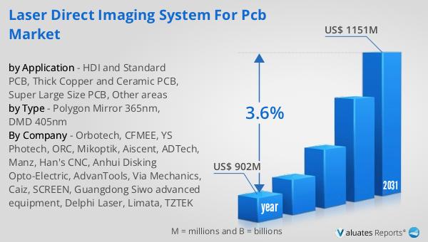
The outlook for the Global Laser Direct Imaging System for PCB Market indicates a promising future, with the market valued at approximately US$ 902 million in 2024 and projected to grow to around US$ 1151 million by 2031. This growth, at a compound annual growth rate (CAGR) of 3.6% during the forecast period, underscores the increasing demand for advanced PCB manufacturing technologies. One of the key advantages of LDI systems is the elimination of the need for a photo-tool, which traditionally posed challenges such as alignment issues, light refraction problems, and imperfections due to environmental variations. By removing these obstacles, LDI systems enhance the precision and efficiency of the PCB manufacturing process, leading to higher quality products and reduced production costs. The market is characterized by a high level of concentration, with the top five players accounting for approximately 70% of the global market share. This indicates a competitive landscape where leading companies are leveraging their technological expertise and market presence to maintain their dominance. These companies are likely to continue investing in research and development to further enhance the capabilities of LDI systems, ensuring they remain at the forefront of innovation in the PCB manufacturing industry. As the demand for more sophisticated electronic devices continues to rise, the Global Laser Direct Imaging System for PCB Market is poised to play a crucial role in meeting the evolving needs of the electronics sector.
| Report Metric | Details |
| Report Name | Laser Direct Imaging System for PCB Market |
| Accounted market size in year | US$ 902 million |
| Forecasted market size in 2031 | US$ 1151 million |
| CAGR | 3.6% |
| Base Year | year |
| Forecasted years | 2025 - 2031 |
| by Type |
|
| by Application |
|
| Production by Region |
|
| Consumption by Region |
|
| By Company | Orbotech, CFMEE, YS Photech, ORC, Mikoptik, Aiscent, ADTech, Manz, Han's CNC, Anhui Disking Opto-Electric, AdvanTools, Via Mechanics, Caiz, SCREEN, Guangdong Siwo advanced equipment, Delphi Laser, Limata, TZTEK |
| Forecast units | USD million in value |
| Report coverage | Revenue and volume forecast, company share, competitive landscape, growth factors and trends |


