What is Global 4 Inches GaN Single Crystal Substrate Market?
The Global 4 Inches GaN Single Crystal Substrate Market is a specialized segment within the semiconductor industry that focuses on the production and distribution of gallium nitride (GaN) substrates, specifically those that are four inches in diameter. GaN is a semiconductor material that has gained significant attention due to its superior properties, such as high thermal conductivity, high breakdown voltage, and high electron mobility, making it ideal for high-power and high-frequency applications. The four-inch size is particularly important as it represents a balance between cost-effectiveness and performance, allowing for the production of larger wafers that can be used in a variety of electronic devices. This market is driven by the increasing demand for efficient and compact electronic components in industries such as telecommunications, automotive, and consumer electronics. As technology advances, the need for substrates that can support higher power densities and frequencies continues to grow, positioning the Global 4 Inches GaN Single Crystal Substrate Market as a critical component in the future of electronics manufacturing. The market is characterized by ongoing research and development efforts aimed at improving the quality and reducing the cost of GaN substrates, which are essential for the widespread adoption of GaN-based technologies.
4 Inch GaN wafers (non-doped), 4 Inch GaN wafers (iron doped) in the Global 4 Inches GaN Single Crystal Substrate Market:
4 Inch GaN wafers are a crucial part of the Global 4 Inches GaN Single Crystal Substrate Market, and they come in two primary types: non-doped and iron-doped. Non-doped 4 Inch GaN wafers are pure GaN substrates that have not been intentionally infused with any additional elements. These wafers are highly valued for their excellent electrical properties, making them suitable for a wide range of applications, particularly in high-frequency and high-power electronic devices. The absence of doping elements ensures that the intrinsic properties of GaN are preserved, allowing for optimal performance in devices that require high electron mobility and thermal stability. On the other hand, 4 Inch GaN wafers that are iron-doped have been intentionally infused with iron atoms during the manufacturing process. This doping process is used to modify the electrical properties of the GaN substrate, often to increase its resistivity. Iron-doped GaN wafers are particularly useful in applications where high resistivity is required, such as in certain types of power electronic devices. The addition of iron helps to suppress the parasitic conduction paths that can occur in non-doped GaN, thereby enhancing the performance of devices that operate under high voltage conditions. Both types of wafers play a significant role in the market, catering to different needs and applications. The choice between non-doped and iron-doped GaN wafers depends largely on the specific requirements of the application, such as the desired electrical characteristics and the operating environment. As the demand for more efficient and compact electronic devices continues to grow, the development and production of both non-doped and iron-doped 4 Inch GaN wafers are expected to expand, driven by advancements in manufacturing technologies and the increasing adoption of GaN-based solutions across various industries. The versatility and superior performance of GaN wafers make them an attractive option for manufacturers looking to enhance the capabilities of their electronic products. As a result, the Global 4 Inches GaN Single Crystal Substrate Market is poised for significant growth, with both non-doped and iron-doped wafers playing a pivotal role in the evolution of modern electronics.
Laser Diodes, Power Electronic Devices, High Frequency Electronic Devices, Others in the Global 4 Inches GaN Single Crystal Substrate Market:
The Global 4 Inches GaN Single Crystal Substrate Market finds its usage in several key areas, including laser diodes, power electronic devices, high-frequency electronic devices, and other applications. In the realm of laser diodes, GaN substrates are essential due to their ability to support high-power and high-frequency operations. Laser diodes made from GaN are used in a variety of applications, such as optical storage devices, laser printers, and medical equipment. The high thermal conductivity and electron mobility of GaN substrates ensure that laser diodes can operate efficiently and reliably, even under demanding conditions. In power electronic devices, GaN substrates are increasingly being used to replace traditional silicon-based components. The superior properties of GaN, such as higher breakdown voltage and thermal stability, allow for the development of power devices that are more efficient and compact. This is particularly important in applications such as electric vehicles, renewable energy systems, and power supplies, where efficiency and size are critical factors. High-frequency electronic devices also benefit from the use of GaN substrates. The high electron mobility of GaN allows for the development of devices that can operate at higher frequencies than those made from traditional materials. This makes GaN-based devices ideal for use in telecommunications, radar systems, and satellite communications, where high-frequency performance is essential. In addition to these specific applications, GaN substrates are also used in a variety of other areas, such as sensors, LEDs, and RF amplifiers. The versatility of GaN substrates makes them an attractive option for manufacturers looking to enhance the performance and efficiency of their products. As the demand for more advanced electronic devices continues to grow, the Global 4 Inches GaN Single Crystal Substrate Market is expected to expand, driven by the increasing adoption of GaN-based solutions across various industries. The unique properties of GaN substrates make them a critical component in the development of next-generation electronic devices, and their usage is likely to increase as technology continues to evolve.
Global 4 Inches GaN Single Crystal Substrate Market Outlook:
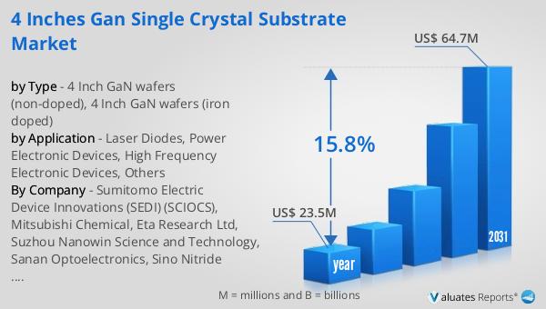
The outlook for the Global 4 Inches GaN Single Crystal Substrate Market is promising, with significant growth expected in the coming years. In 2024, the market was valued at approximately $23.5 million, reflecting the increasing demand for GaN substrates in various high-tech applications. By 2031, the market is projected to reach a revised size of around $64.7 million, indicating a robust compound annual growth rate (CAGR) of 15.8% during the forecast period. This growth is driven by the expanding use of GaN substrates in industries such as telecommunications, automotive, and consumer electronics, where the need for efficient and compact electronic components is paramount. The superior properties of GaN, such as high thermal conductivity, high breakdown voltage, and high electron mobility, make it an ideal material for high-power and high-frequency applications. As technology continues to advance, the demand for substrates that can support higher power densities and frequencies is expected to increase, further fueling the growth of the Global 4 Inches GaN Single Crystal Substrate Market. The market is characterized by ongoing research and development efforts aimed at improving the quality and reducing the cost of GaN substrates, which are essential for the widespread adoption of GaN-based technologies. As a result, the Global 4 Inches GaN Single Crystal Substrate Market is poised for significant growth, with both non-doped and iron-doped wafers playing a pivotal role in the evolution of modern electronics.
| Report Metric | Details |
| Report Name | 4 Inches GaN Single Crystal Substrate Market |
| Accounted market size in year | US$ 23.5 million |
| Forecasted market size in 2031 | US$ 64.7 million |
| CAGR | 15.8% |
| Base Year | year |
| Forecasted years | 2025 - 2031 |
| by Type |
|
| by Application |
|
| Production by Region |
|
| Consumption by Region |
|
| By Company | Sumitomo Electric Device Innovations (SEDI) (SCIOCS), Mitsubishi Chemical, Eta Research Ltd, Suzhou Nanowin Science and Technology, Sanan Optoelectronics, Sino Nitride Semiconductor, Goetsu Semiconductor Wuxi, BTOZ, Toyoda Gosei, Kyma Technologies |
| Forecast units | USD million in value |
| Report coverage | Revenue and volume forecast, company share, competitive landscape, growth factors and trends |