What is Global Wafer UV Film and Non-UV Film (Blue Film) Market?
The global Wafer UV Film and Non-UV Film (Blue Film) market is a specialized segment within the semiconductor industry, focusing on protective films used during the manufacturing process of semiconductor wafers. These films are crucial in ensuring the integrity and quality of wafers during various stages of production, such as back grinding and wafer dicing. UV films are designed to be sensitive to ultraviolet light, allowing them to be easily removed after processing, while Non-UV films, often referred to as Blue Films, do not have this sensitivity and are used for different protective purposes. The market for these films is driven by the increasing demand for semiconductors in various applications, including consumer electronics, automotive, and industrial sectors. As technology advances, the need for more precise and reliable wafer processing techniques grows, further fueling the demand for high-quality protective films. The market is characterized by continuous innovation and development to meet the evolving needs of the semiconductor industry, ensuring that the films provide optimal protection without compromising the efficiency of the manufacturing process.
UV Film, Non-UV Film in the Global Wafer UV Film and Non-UV Film (Blue Film) Market:
UV films are essential in the semiconductor manufacturing process due to their unique properties. These films are sensitive to ultraviolet light, which allows them to be easily removed after the wafer processing stages. This feature is particularly useful in applications where the film needs to be removed without leaving any residue, ensuring the wafer's surface remains pristine. UV films are commonly used in back grinding and wafer dicing processes. During back grinding, the wafer is thinned to the desired thickness, and the UV film protects the wafer's surface from damage. Once the grinding process is complete, the film can be exposed to UV light, making it easy to peel off without damaging the wafer. In wafer dicing, UV films provide a protective layer that prevents chipping and cracking during the cutting process. The film's ability to be removed cleanly after dicing ensures that the wafers are ready for the next stage of production without any additional cleaning steps. Non-UV films, or Blue Films, serve a different purpose in the semiconductor manufacturing process. These films are not sensitive to ultraviolet light and are used in applications where the film does not need to be removed as cleanly or quickly. Blue Films are often used in situations where long-term protection is required, such as during storage or transportation of wafers. They provide a durable barrier that protects the wafer from physical damage and contamination. The choice between UV and Non-UV films depends on the specific requirements of the manufacturing process and the desired outcome. Both types of films play a crucial role in ensuring the quality and reliability of semiconductor wafers, contributing to the overall efficiency and effectiveness of the production process.
Back Grinding, Wafer Dicing in the Global Wafer UV Film and Non-UV Film (Blue Film) Market:
The usage of Global Wafer UV Film and Non-UV Film (Blue Film) in back grinding and wafer dicing processes is critical to the semiconductor manufacturing industry. In back grinding, the wafer is thinned to achieve the desired thickness, which is essential for the production of various semiconductor devices. During this process, the wafer is subjected to significant mechanical stress, which can lead to damage if not properly protected. UV films are used to cover the wafer's surface, providing a protective barrier that absorbs the stress and prevents damage. Once the grinding process is complete, the UV film can be exposed to ultraviolet light, causing it to lose its adhesive properties and allowing it to be easily removed without leaving any residue. This ensures that the wafer remains intact and ready for the next stage of production. In wafer dicing, the wafer is cut into individual semiconductor chips. This process involves precise and delicate cutting, which can cause chipping and cracking if the wafer is not adequately protected. UV films are applied to the wafer's surface before dicing, providing a protective layer that absorbs the mechanical stress and prevents damage. After the dicing process is complete, the UV film can be exposed to ultraviolet light, making it easy to peel off without damaging the individual chips. Non-UV films, or Blue Films, are also used in wafer dicing, particularly in situations where long-term protection is required. These films provide a durable barrier that protects the wafer from physical damage and contamination during storage and transportation. The choice between UV and Non-UV films depends on the specific requirements of the manufacturing process and the desired outcome. Both types of films play a crucial role in ensuring the quality and reliability of semiconductor wafers, contributing to the overall efficiency and effectiveness of the production process.
Global Wafer UV Film and Non-UV Film (Blue Film) Market Outlook:
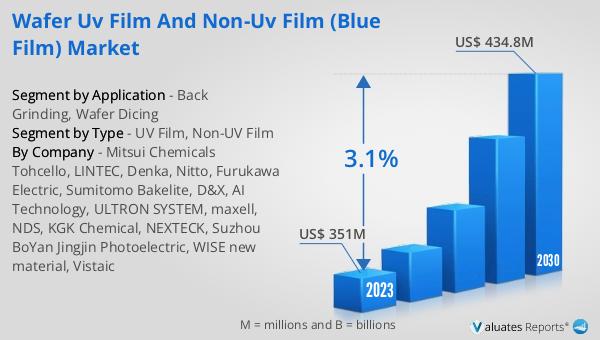
The global Wafer UV Film and Non-UV Film (Blue Film) market was valued at US$ 351 million in 2023 and is anticipated to reach US$ 434.8 million by 2030, witnessing a CAGR of 3.1% during the forecast period 2024-2030. The largest region, Asia Pacific, experienced a decline of 2.0 percent. Sales in the Americas were US$142.1 billion, up 17.0% year-on-year, while sales in Europe were US$53.8 billion, up 12.6% year-on-year. Sales in Japan were US$48.1 billion, marking a 10.0% year-on-year increase. However, sales in the largest Asia-Pacific region were US$336.2 billion, down 2.0% year-on-year. This market outlook highlights the varying performance across different regions, with significant growth observed in the Americas, Europe, and Japan, while the Asia-Pacific region faced a slight decline. The overall market growth is driven by the increasing demand for semiconductors in various applications, including consumer electronics, automotive, and industrial sectors. The continuous innovation and development in wafer processing techniques further fuel the demand for high-quality protective films, ensuring the integrity and quality of semiconductor wafers during manufacturing.
| Report Metric | Details |
| Report Name | Wafer UV Film and Non-UV Film (Blue Film) Market |
| Accounted market size in 2023 | US$ 351 million |
| Forecasted market size in 2030 | US$ 434.8 million |
| CAGR | 3.1% |
| Base Year | 2023 |
| Forecasted years | 2024 - 2030 |
| Segment by Type |
|
| Segment by Application |
|
| Production by Region |
|
| Consumption by Region |
|
| By Company | Mitsui Chemicals Tohcello, LINTEC, Denka, Nitto, Furukawa Electric, Sumitomo Bakelite, D&X, AI Technology, ULTRON SYSTEM, maxell, NDS, KGK Chemical, NEXTECK, Suzhou BoYan Jingjin Photoelectric, WISE new material, Vistaic |
| Forecast units | USD million in value |
| Report coverage | Revenue and volume forecast, company share, competitive landscape, growth factors and trends |


