What is Global Advanced Packaging Metrology Inspection Equipment Market?
The Global Advanced Packaging Metrology Inspection Equipment Market is a specialized sector within the broader semiconductor industry, focusing on the tools and technologies used to measure and ensure the quality and reliability of advanced packaging processes. Advanced packaging refers to a set of techniques used to mount and interconnect semiconductor devices to enhance their performance, power efficiency, and reduce their size. As these semiconductor devices become more complex, with smaller features and more layers, the need for precise metrology and inspection equipment becomes critical. This market encompasses a range of equipment designed to perform detailed inspections and measurements at various stages of the packaging process, from wafer level to the final packaged product. The equipment helps in identifying defects, ensuring alignment, measuring critical dimensions, and verifying the integrity of the materials used, thereby ensuring the functionality and reliability of the semiconductor devices. The demand for such equipment is driven by the continuous advancements in semiconductor technology, the increasing complexity of integrated circuits, and the need for higher performance and miniaturization in electronic devices.
Optical Based Type, Infrared Type in the Global Advanced Packaging Metrology Inspection Equipment Market:
Optical Based Type and Infrared Type are two pivotal technologies underpinning the Global Advanced Packaging Metrology Inspection Equipment Market, each playing a crucial role in ensuring the precision and efficiency of semiconductor packaging. Optical Based Type metrology equipment utilizes light, typically in the visible spectrum, to measure and inspect the dimensions, alignments, and defects in semiconductor packages. This technology is highly versatile and can be adapted to various inspection tasks, from surface topography and layer thickness measurements to defect detection and pattern recognition. Its non-contact nature allows for rapid inspections without risking damage to the delicate semiconductor devices. On the other hand, Infrared Type metrology equipment employs infrared light to penetrate materials that are opaque to visible light, enabling the inspection of internal structures and features within semiconductor packages. This capability is particularly valuable for inspecting underfill, die attachment, and other internal package components, which are critical for the device's performance and reliability. Both technologies complement each other, with Optical Based Type providing detailed surface inspections and Infrared Type offering insights into hidden structures, together ensuring the comprehensive quality control of advanced semiconductor packages. The continuous evolution of these technologies, driven by the relentless pursuit of smaller, faster, and more efficient electronic devices, underscores their importance in the Global Advanced Packaging Metrology Inspection Equipment Market.
IDM, Foundry in the Global Advanced Packaging Metrology Inspection Equipment Market:
In the realms of Integrated Device Manufacturers (IDM) and Foundries, the Global Advanced Packaging Metrology Inspection Equipment Market plays a pivotal role in enhancing the quality, reliability, and performance of semiconductor devices. IDMs, companies that design and manufacture their semiconductor products, rely heavily on advanced packaging metrology inspection equipment to ensure that their in-house developed devices meet the stringent standards required for performance and reliability. This equipment enables IDMs to conduct thorough inspections and measurements at various stages of the packaging process, identifying defects and verifying critical dimensions to ensure that the final product performs as intended. On the other hand, Foundries, which are companies that manufacture semiconductor devices on behalf of other companies, use this equipment to guarantee the quality and reliability of the products they produce. Given the competitive nature of the semiconductor industry and the complex requirements of their clients, foundries must maintain the highest standards of quality control. Advanced packaging metrology inspection equipment allows them to achieve this by providing precise and accurate measurements, ensuring that every device they produce meets the exact specifications of their clients. The usage of this equipment in both IDMs and Foundries underscores its importance in the semiconductor manufacturing process, where precision, reliability, and efficiency are paramount.
Global Advanced Packaging Metrology Inspection Equipment Market Outlook:
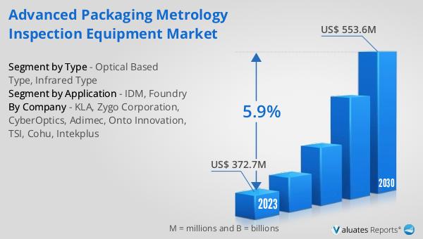
The market outlook for the Global Advanced Packaging Metrology Inspection Equipment Market presents a promising future, with its valuation at approximately 372.7 million US dollars in 2023, and projections suggesting a growth to about 553.6 million US dollars by the year 2030. This anticipated growth, representing a Compound Annual Growth Rate (CAGR) of 5.9% throughout the forecast period from 2024 to 2030, highlights the increasing demand and significance of advanced packaging metrology inspection equipment in the semiconductor industry. The market's expansion is further evidenced by the substantial market share held by North America, Europe, and Japan, which collectively account for 23% of the global market. This data underscores the critical role that advanced packaging metrology inspection equipment plays in the development and manufacturing of semiconductor devices, driven by the continuous advancements in technology and the growing need for more sophisticated, reliable, and miniaturized electronic components. The market's robust growth prospects reflect the industry's response to these evolving demands, ensuring the ongoing enhancement of semiconductor device quality and performance through precise and efficient inspection and metrology processes.
| Report Metric | Details |
| Report Name | Advanced Packaging Metrology Inspection Equipment Market |
| Accounted market size in 2023 | US$ 372.7 million |
| Forecasted market size in 2030 | US$ 553.6 million |
| CAGR | 5.9% |
| Base Year | 2023 |
| Forecasted years | 2024 - 2030 |
| Segment by Type |
|
| Segment by Application |
|
| Production by Region |
|
| Consumption by Region |
|
| By Company | KLA, Zygo Corporation, CyberOptics, Adimec, Onto Innovation, TSI, Cohu, Intekplus |
| Forecast units | USD million in value |
| Report coverage | Revenue and volume forecast, company share, competitive landscape, growth factors and trends |


