What is Global Through Glass Via (TGV) Glass Wafer Market?
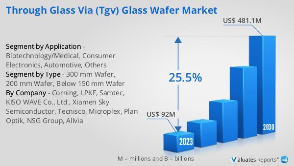
The Global Through Glass Via (TGV) Glass Wafer Market is an intriguing sector that focuses on the production and utilization of glass wafers with through-glass vias. These are essentially microscopic holes drilled into the glass wafers, allowing for electrical connections to pass through them. This technology is pivotal in the miniaturization and enhancement of electronic devices, offering a robust platform for various applications in electronics and photonics. The market's significance stems from its ability to provide solutions that traditional silicon-based technologies cannot, particularly in terms of insulation properties and the facilitation of high-frequency applications. As of 2023, the market has been valued at US$ 92 million, and with the advancements in technology and increasing demand for sophisticated electronic components, it is projected to soar to US$ 481.1 million by 2030. This remarkable growth trajectory, marked by a compound annual growth rate (CAGR) of 25.5% during the forecast period from 2024 to 2030, underscores the market's potential and the industry's recognition of TGV glass wafers' unique benefits. The market is also characterized by a competitive landscape where the top three players command about 50% of the market share, highlighting a concentrated yet dynamic market environment.
300 mm Wafer, 200 mm Wafer, Below 150 mm Wafer in the Global Through Glass Via (TGV) Glass Wafer Market:
Diving into the specifics of the Global Through Glass Via (TGV) Glass Wafer Market, it's essential to understand the categorization based on wafer sizes, which include 300 mm, 200 mm, and below 150 mm wafers. Each category serves distinct segments of the electronics and photonics industries, catering to different requirements in terms of device miniaturization, performance, and application. The 300 mm wafers, being the largest, are primarily used in applications requiring a larger surface area for more complex or higher volume circuitry. This size is particularly prevalent in the manufacturing of high-performance computing devices and large-scale photonics applications. On the other hand, the 200 mm wafers strike a balance between size and functionality, making them suitable for a wide range of consumer electronics and automotive applications where space is a consideration but performance cannot be compromised. Lastly, the wafers that measure below 150 mm are tailored for specialized applications where compact size is paramount. These smaller wafers are often utilized in biomedical devices, advanced sensors, and other niche applications where the unique properties of glass, such as its bio-compatibility and superior insulating characteristics, are crucial. The differentiation in wafer sizes allows the TGV Glass Wafer Market to cater to a broad spectrum of technological needs, ensuring that various sectors can leverage the advantages of glass wafers in their product development and innovation efforts.
Biotechnology/Medical, Consumer Electronics, Automotive, Others in the Global Through Glass Via (TGV) Glass Wafer Market:
The application of the Global Through Glass Via (TGV) Glass Wafer Market spans several critical sectors, including biotechnology/medical, consumer electronics, automotive, and others, showcasing the technology's versatility and broad appeal. In the biotechnology and medical fields, TGV glass wafers are revolutionizing the development of lab-on-a-chip devices and other miniaturized diagnostic tools, offering unprecedented precision and reliability. Their inherent biocompatibility makes them ideal for such applications, where glass's non-reactive nature ensures that there is no interference with biological samples. In the realm of consumer electronics, these wafers are integral to the production of compact, high-performance devices such as smartphones, tablets, and wearable technology. Their ability to facilitate high-density, through-glass interconnections allows for the design of thinner, more efficient devices without compromising on functionality. The automotive sector benefits from TGV glass wafers in the development of advanced sensors and control systems, contributing to the enhancement of vehicle safety, performance, and connectivity. Other applications include aerospace, where the technology's reliability and resistance to harsh environments are invaluable, and telecommunications, where glass wafers enable the production of high-frequency, high-speed communication components. This wide-ranging utility underscores the TGV Glass Wafer Market's role in driving innovation across multiple industries, making it a cornerstone of modern technological advancement.
Global Through Glass Via (TGV) Glass Wafer Market Outlook:
The market outlook for the Global Through Glass Via (TGV) Glass Wafer Market presents a promising future, with the sector's valuation at US$ 92 million in 2023, set to escalate to US$ 481.1 million by 2030. This projection indicates a robust compound annual growth rate (CAGR) of 25.5% from 2024 to 2030, reflecting the market's dynamic growth potential. Such an optimistic forecast can be attributed to the increasing adoption of TGV glass wafer technology across various industries, driven by the demand for more sophisticated and miniaturized electronic components. The technology's unique ability to provide high-density interconnections in a compact form factor is particularly appealing in an era where electronic devices are becoming increasingly smaller yet more powerful. Additionally, the market's competitive landscape, where the top three players hold about 50% of the market share, suggests a healthy level of competition and innovation within the industry. This competitive environment not only fosters technological advancements but also ensures that the benefits of TGV glass wafer technology are accessible to a wide range of applications, from consumer electronics to automotive and medical devices. The market's growth is a testament to the technology's versatility and its capacity to meet the evolving needs of modern electronics and photonics.
| Report Metric | Details |
| Report Name | Through Glass Via (TGV) Glass Wafer Market |
| Accounted market size in 2023 | US$ 92 million |
| Forecasted market size in 2030 | US$ 481.1 million |
| CAGR | 25.5% |
| Base Year | 2023 |
| Forecasted years | 2024 - 2030 |
| Segment by Type |
|
| Segment by Application |
|
| Production by Region |
|
| Consumption by Region |
|
| By Company | Corning, LPKF, Samtec, KISO WAVE Co., Ltd., Xiamen Sky Semiconductor, Tecnisco, Microplex, Plan Optik, NSG Group, Allvia |
| Forecast units | USD million in value |
| Report coverage | Revenue and volume forecast, company share, competitive landscape, growth factors and trends |