What is Global Sputtering Targets for Thin-Film Deposition Market?
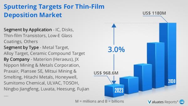
The Global Sputtering Targets for Thin-Film Deposition Market is a specialized sector within the materials science and semiconductor industries, focusing on the production and distribution of sputtering targets used in the thin-film deposition process. This process is critical for creating thin films of material on substrates, which is a foundational technique in manufacturing a wide range of electronic and optical components. The market's value was pegged at US$ 968.6 million in 2023 and is projected to climb to US$ 1180 million by 2030, growing at a compound annual growth rate (CAGR) of 3.0% during the forecast period from 2024 to 2030. This growth is reflective of the increasing demand for thin-film technologies in various applications, including semiconductors, photovoltaic cells, and display technologies. The expansion of the market is further supported by the broader semiconductor industry, which itself is on a growth trajectory from US$ 579 billion in 2022 to an expected US$ 790 billion by 2029, marking a CAGR of 6%. Despite a 2.0% decline in the Asia Pacific region, the largest market for these technologies, other regions like the Americas, Europe, and Japan have seen significant year-on-year growth, underscoring the global nature of the demand for sputtering targets and thin-film deposition technologies.
Metal Target, Alloy Target, Ceramic Compound Target in the Global Sputtering Targets for Thin-Film Deposition Market:
Diving into the specifics, the Global Sputtering Targets for Thin-Film Deposition Market is segmented into metal targets, alloy targets, and ceramic compound targets, each serving unique roles in the fabrication of thin films. Metal targets, composed of pure metals, are widely used due to their conductive properties, making them ideal for electronic and electrical applications. Alloy targets, on the other hand, are a blend of two or more metals, designed to combine the properties of the constituent metals to meet specific film characteristics such as enhanced durability or improved electrical conductivity. Ceramic compound targets comprise a mix of metallic and non-metallic elements and are favored for their high resistance to heat and corrosion, making them suitable for applications in harsh environments. These targets find their applications across a broad spectrum of industries, including semiconductor manufacturing, data storage devices, display technologies, and photovoltaic cells, among others. The choice of target material is dictated by the desired properties of the thin film, which in turn depends on the end-use application. The market for these targets is driven by technological advancements, the growing demand for high-performance materials, and the expanding range of applications for thin films. The development of new materials and deposition techniques continues to open new avenues for the application of sputtering targets, further propelling the market's growth.
IC, Disks, Thin-film Transistors, Low-E Glass Coatings, Others in the Global Sputtering Targets for Thin-Film Deposition Market:
The usage of the Global Sputtering Targets for Thin-Film Deposition Market spans several key areas, including Integrated Circuits (IC), Disks, Thin-film Transistors (TFTs), Low-Emissivity (Low-E) Glass Coatings, and other applications. In the realm of ICs, sputtering targets are crucial for depositing thin films of conductive materials onto silicon wafers, a fundamental step in semiconductor device fabrication. For Disks, particularly in data storage devices like hard disk drives, sputtering targets are used to deposit magnetic layers that store data. Thin-film Transistors, which are essential components of liquid crystal displays (LCDs) and organic light-emitting diode (OLED) displays, rely on thin films of semiconductor materials deposited using sputtering targets to function. Low-E Glass Coatings, which improve the energy efficiency of architectural glass by reflecting infrared light while allowing visible light to pass through, are another application where sputtering targets play a pivotal role. Beyond these applications, sputtering targets are used in a variety of other areas, including but not limited to, coating of tools to improve wear resistance, decorative coatings, and anti-reflective coatings for optical devices. The versatility of sputtering targets and their ability to deposit a wide range of materials make them indispensable in the fabrication of thin films for a multitude of applications.
Global Sputtering Targets for Thin-Film Deposition Market Outlook:
The market outlook for Global Sputtering Targets for Thin-Film Deposition presents a promising growth trajectory, with the market's value estimated at US$ 968.6 million in 2023, expected to ascend to US$ 1180 million by 2030, marking a CAGR of 3.0% during the forecast period from 2024 to 2030. This growth is reflective of the burgeoning demand across various sectors for thin-film technologies, a cornerstone in the manufacturing of electronic and optical components. Parallelly, the semiconductor industry, a significant consumer of sputtering targets, is witnessing robust expansion, projected to grow from US$ 579 billion in 2022 to US$ 790 billion by 2029, at a CAGR of 6%. Despite a slight downturn in the Asia Pacific region, the largest market for these technologies, other regions have demonstrated substantial growth. The Americas, Europe, and Japan have reported year-on-year sales increases of 17.0%, 12.6%, and 10.0%, respectively, highlighting the widespread and growing demand for sputtering targets and thin-film deposition technologies globally. This outlook underscores the critical role of sputtering targets in the advancement of thin-film technologies and their broad application across various industries.
| Report Metric | Details |
| Report Name | Sputtering Targets for Thin-Film Deposition Market |
| Accounted market size in 2023 | US$ 968.6 million |
| Forecasted market size in 2030 | US$ 1180 million |
| CAGR | 3.0% |
| Base Year | 2023 |
| Forecasted years | 2024 - 2030 |
| Segment by Type |
|
| Segment by Application |
|
| Production by Region |
|
| Consumption by Region |
|
| By Company | Materion (Heraeus), JX Nippon Mining & Metals Corporation, Praxair, Plansee SE, Mitsui Mining & Smelting, Hitachi Metals, Honeywell, Sumitomo Chemical, ULVAC, TOSOH, Ningbo Jiangfeng, Luvata, Heesung, Fujian Acetron New Materials Co., Ltd, Luoyang Sifon Electronic Materials, GRIKIN Advanced Material Co., Ltd., Umicore Thin Film Products, FURAYA Metals Co., Ltd, Advantec, Angstrom Sciences, Changzhou Sujing ElectronicMaterial |
| Forecast units | USD million in value |
| Report coverage | Revenue and volume forecast, company share, competitive landscape, growth factors and trends |


