What is Global Thermoelectric Semiconductor Market?
The Global Thermoelectric Semiconductor Market is a fascinating and rapidly evolving sector that plays a crucial role in various industries. Thermoelectric semiconductors are materials that can convert temperature differences directly into electrical voltage and vice versa. This unique property makes them highly valuable for applications in power generation and cooling systems. The market for these semiconductors is driven by the increasing demand for energy-efficient solutions and the growing focus on sustainable technologies. As industries strive to reduce their carbon footprint and enhance energy efficiency, thermoelectric semiconductors offer a promising solution. They are used in a wide range of applications, from consumer electronics to automotive and industrial sectors, providing both cooling and power generation capabilities. The market is characterized by continuous advancements in material science and technology, leading to improved performance and efficiency of thermoelectric devices. As a result, the Global Thermoelectric Semiconductor Market is expected to witness significant growth in the coming years, driven by the increasing adoption of these innovative materials across various industries.
Single Stage Module, Multistage Module in the Global Thermoelectric Semiconductor Market:
In the realm of the Global Thermoelectric Semiconductor Market, Single Stage Modules and Multistage Modules represent two distinct approaches to harnessing the power of thermoelectric technology. Single Stage Modules are the simpler of the two, consisting of a single layer of thermoelectric material sandwiched between two ceramic plates. These modules are designed to handle moderate temperature differences and are typically used in applications where space and cost are critical considerations. They are ideal for consumer electronics, where compact size and efficiency are paramount. Single Stage Modules are often employed in devices like portable coolers, personal electronics, and small-scale power generation systems. Their straightforward design allows for easy integration into existing systems, making them a popular choice for manufacturers looking to enhance the energy efficiency of their products. On the other hand, Multistage Modules are more complex and are designed to handle larger temperature gradients. These modules consist of multiple layers of thermoelectric materials stacked together, allowing them to achieve higher levels of cooling or power generation. Multistage Modules are commonly used in applications that require significant temperature control, such as telecommunications equipment, medical devices, and industrial machinery. The ability to manage larger temperature differences makes them suitable for high-performance applications where precision and reliability are crucial. In the telecommunications industry, for example, Multistage Modules are used to maintain optimal operating temperatures for sensitive equipment, ensuring consistent performance and longevity. Similarly, in the medical field, these modules are employed in devices that require precise temperature regulation, such as laboratory equipment and diagnostic machines. The automotive industry also benefits from the capabilities of Multistage Modules, particularly in electric and hybrid vehicles where efficient thermal management is essential for battery performance and longevity. By effectively managing the temperature of critical components, these modules help enhance the overall efficiency and reliability of automotive systems. In summary, both Single Stage and Multistage Modules play vital roles in the Global Thermoelectric Semiconductor Market, catering to different needs and applications. While Single Stage Modules offer simplicity and cost-effectiveness for moderate temperature control, Multistage Modules provide advanced capabilities for high-performance applications. As the demand for energy-efficient and sustainable solutions continues to grow, the development and adoption of these modules are expected to expand, driving further innovation and growth in the thermoelectric semiconductor market.
Consumer Electronics, Telecommunications, Automotive, Mining and Power Generation, Others in the Global Thermoelectric Semiconductor Market:
The Global Thermoelectric Semiconductor Market finds extensive usage across various sectors, each benefiting from the unique properties of thermoelectric materials. In the realm of Consumer Electronics, thermoelectric semiconductors are employed to enhance the energy efficiency and performance of devices. They are used in cooling systems for laptops, smartphones, and other portable electronics, ensuring optimal operating temperatures and prolonging the lifespan of these devices. By maintaining efficient thermal management, thermoelectric semiconductors help prevent overheating, which can lead to reduced performance and potential damage. In the Telecommunications sector, thermoelectric semiconductors play a crucial role in maintaining the reliability and performance of communication equipment. They are used to regulate the temperature of sensitive components, such as transceivers and amplifiers, ensuring consistent signal quality and preventing thermal-related failures. The ability to manage temperature effectively is vital in telecommunications, where equipment operates continuously and is often exposed to varying environmental conditions. In the Automotive industry, thermoelectric semiconductors are used for both cooling and power generation applications. They are employed in climate control systems to provide efficient heating and cooling, enhancing passenger comfort while reducing energy consumption. Additionally, thermoelectric generators are used to convert waste heat from the engine into electrical energy, improving overall fuel efficiency and reducing emissions. The Mining and Power Generation sectors also benefit from the capabilities of thermoelectric semiconductors. In mining operations, these materials are used to power remote sensors and monitoring equipment, providing reliable energy sources in challenging environments. In power generation, thermoelectric semiconductors are used to convert waste heat from industrial processes into usable electricity, contributing to energy recovery and sustainability efforts. Beyond these specific industries, thermoelectric semiconductors find applications in various other fields, including aerospace, healthcare, and industrial automation. Their versatility and efficiency make them valuable for any application requiring precise temperature control or energy conversion. As industries continue to prioritize energy efficiency and sustainability, the demand for thermoelectric semiconductors is expected to grow, driving further innovation and adoption across diverse sectors.
Global Thermoelectric Semiconductor Market Outlook:
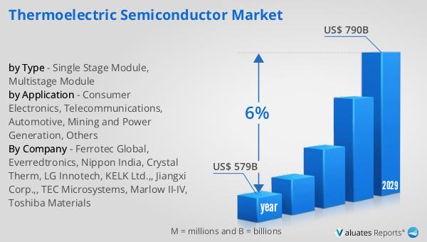
The global semiconductor market, valued at approximately $579 billion in 2022, is on a trajectory to reach around $790 billion by 2029, reflecting a compound annual growth rate (CAGR) of 6% over the forecast period. This growth is indicative of the increasing demand for semiconductors across various industries, driven by advancements in technology and the rising need for energy-efficient solutions. Semiconductors are the backbone of modern electronics, powering everything from smartphones and computers to advanced industrial machinery and automotive systems. The market's expansion is fueled by the continuous development of new applications and the integration of semiconductors into emerging technologies such as artificial intelligence, the Internet of Things (IoT), and 5G networks. As industries strive to enhance performance and efficiency, the demand for high-quality semiconductors is expected to rise, contributing to the market's growth. Additionally, the push for sustainable and energy-efficient solutions is driving innovation in semiconductor materials and design, further propelling the market forward. The projected growth of the semiconductor market underscores its critical role in shaping the future of technology and its impact on various sectors of the global economy.
| Report Metric | Details |
| Report Name | Thermoelectric Semiconductor Market |
| Accounted market size in year | US$ 579 billion |
| Forecasted market size in 2029 | US$ 790 billion |
| CAGR | 6% |
| Base Year | year |
| Forecasted years | 2025 - 2029 |
| by Type |
|
| by Application |
|
| Production by Region |
|
| Consumption by Region |
|
| By Company | Ferrotec Global, Everredtronics, Nippon India, Crystal Therm, LG Innotech, KELK Ltd.,, Jiangxi Corp.,, TEC Microsystems, Marlow II-IV, Toshiba Materials |
| Forecast units | USD million in value |
| Report coverage | Revenue and volume forecast, company share, competitive landscape, growth factors and trends |