What is Global 3D IC and 2.5D IC Packaging Market?
The Global 3D IC and 2.5D IC Packaging Market represents a significant advancement in semiconductor technology, focusing on the integration of multiple integrated circuits (ICs) into a single package. This market is driven by the need for more efficient, compact, and high-performance electronic devices. 3D IC packaging involves stacking silicon wafers or dies and interconnecting them vertically, which enhances performance and reduces power consumption. On the other hand, 2.5D IC packaging uses an interposer, a piece of silicon or another material, to connect multiple dies side by side. This method offers a balance between performance and cost, making it suitable for various applications. The market is expanding due to the increasing demand for miniaturized devices, improved performance, and energy efficiency in consumer electronics, telecommunications, and automotive sectors. The integration of these technologies is crucial for the development of advanced computing systems, offering significant improvements in speed and functionality. As industries continue to push the boundaries of technology, the Global 3D IC and 2.5D IC Packaging Market is poised to play a pivotal role in shaping the future of electronics.
3D Wafer-level Chip-scale Packaging, 3D TSV, 2.5D in the Global 3D IC and 2.5D IC Packaging Market:
3D Wafer-level Chip-scale Packaging (WLCSP), 3D Through-Silicon Via (TSV), and 2.5D IC technologies are at the forefront of the Global 3D IC and 2.5D IC Packaging Market, each offering unique advantages and applications. 3D WLCSP is a packaging technology that allows for the miniaturization of electronic components by enabling the integration of multiple chips into a single package. This method is particularly beneficial for mobile devices and other compact electronics, as it reduces the overall footprint while maintaining high performance. The process involves the direct attachment of the die to the printed circuit board (PCB), eliminating the need for traditional packaging methods and thus reducing costs and improving thermal performance.
Logic, Imaging & Optoelectronics, Memory, MEMS/Sensors, LED, Power in the Global 3D IC and 2.5D IC Packaging Market:
3D TSV technology, on the other hand, involves creating vertical electrical connections (vias) through the silicon wafer, allowing for the stacking of multiple dies. This approach significantly enhances the performance of electronic devices by reducing the distance that signals need to travel, thereby increasing speed and reducing power consumption. TSV is particularly advantageous for applications requiring high bandwidth and low latency, such as data centers and high-performance computing. The ability to stack memory and logic components in a single package also opens up new possibilities for advanced computing architectures, enabling more efficient data processing and storage solutions.
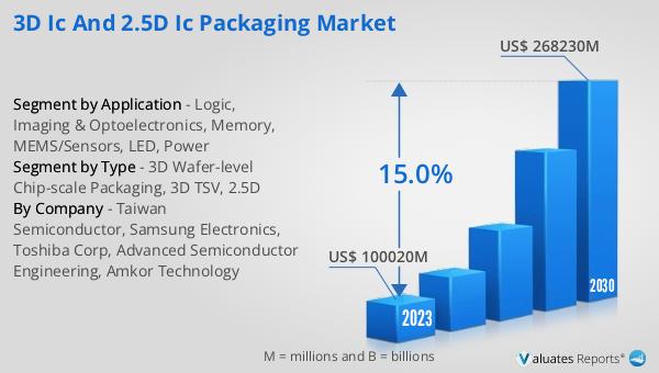
Global 3D IC and 2.5D IC Packaging Market Outlook:
2.5D IC technology, meanwhile, offers a middle ground between traditional 2D packaging and full 3D integration. By using an interposer, 2.5D ICs can connect multiple dies side by side, allowing for increased functionality without the complexity of full 3D stacking. This method is particularly useful for applications that require high performance but are sensitive to cost, such as graphics processing units (GPUs) and field-programmable gate arrays (FPGAs). The use of an interposer also improves thermal management and signal integrity, making 2.5D ICs a popular choice for high-performance computing and telecommunications applications.
| Report Metric | Details |
| Report Name | 3D IC and 2.5D IC Packaging Market |
| Accounted market size in year | US$ 131680 million |
| Forecasted market size in 2031 | US$ 345490 million |
| CAGR | 15.0% |
| Base Year | year |
| Forecasted years | 2025 - 2031 |
| by Type |
|
| by Application |
|
| Production by Region |
|
| Consumption by Region |
|
| By Company | Taiwan Semiconductor, Samsung Electronics, Toshiba Corp, Advanced Semiconductor Engineering, Amkor Technology |
| Forecast units | USD million in value |
| Report coverage | Revenue and volume forecast, company share, competitive landscape, growth factors and trends |


