What is Global UV Objective Lenses for Semiconductor Industry Market?
The Global UV Objective Lenses for the Semiconductor Industry Market is a specialized segment within the broader optical components market, focusing on lenses that are specifically designed to work with ultraviolet (UV) light. These lenses are crucial in the semiconductor industry, where they are used in various inspection and lithography processes. The semiconductor industry relies heavily on precision and accuracy, and UV objective lenses play a vital role in achieving these standards. They are used to focus UV light onto semiconductor wafers during the manufacturing process, enabling the creation of intricate patterns that form the basis of semiconductor devices. The demand for these lenses is driven by the increasing complexity of semiconductor devices and the need for higher precision in manufacturing processes. As technology advances, the semiconductor industry continues to push the boundaries of what is possible, requiring ever more sophisticated equipment, including UV objective lenses. These lenses must be able to withstand the harsh conditions of semiconductor manufacturing environments while maintaining their optical performance. The market for these lenses is expected to grow as the semiconductor industry expands and evolves, driven by the increasing demand for electronic devices and the ongoing miniaturization of semiconductor components.
Max.20x, Max. 20x-50x, Above 50x in the Global UV Objective Lenses for Semiconductor Industry Market:
In the Global UV Objective Lenses for the Semiconductor Industry Market, lenses are categorized based on their magnification capabilities, which are crucial for different applications within the semiconductor manufacturing process. The first category, Max. 20x, includes lenses that offer up to 20 times magnification. These lenses are typically used for applications that require a broader field of view and less magnification, such as initial inspections and general observations of semiconductor wafers. They provide a balance between magnification and field of view, making them suitable for tasks that do not require extremely high levels of detail but still need precision and clarity. The second category, Max. 20x-50x, includes lenses that offer magnification levels between 20 and 50 times. These lenses are used for more detailed inspections where higher magnification is necessary to identify smaller defects or features on semiconductor wafers. They are often used in quality control processes where precision is critical, and any defects could lead to significant issues in the final product. The ability to zoom in on specific areas of a wafer allows for a more thorough inspection and ensures that any potential problems are identified and addressed early in the manufacturing process. The third category, Above 50x, includes lenses that offer magnification levels greater than 50 times. These lenses are used for the most detailed inspections, where even the smallest defects need to be identified and corrected. They are essential in the production of advanced semiconductor devices, where the margin for error is extremely small. These high-magnification lenses allow manufacturers to inspect the intricate patterns and structures on semiconductor wafers, ensuring that they meet the stringent quality standards required in the industry. The use of these lenses is critical in the development of cutting-edge semiconductor technologies, where precision and accuracy are paramount. As the semiconductor industry continues to advance, the demand for high-magnification UV objective lenses is expected to grow, driven by the need for more detailed inspections and the increasing complexity of semiconductor devices. Each category of lenses plays a vital role in the semiconductor manufacturing process, providing the necessary magnification and clarity to ensure that wafers are produced to the highest standards. The choice of lens depends on the specific requirements of the inspection process, with different magnification levels offering different benefits and capabilities. As technology continues to evolve, the development of new and improved UV objective lenses will be essential to meet the changing needs of the semiconductor industry.
Semiconductor Wafer Inspection Equipment, Semiconductor Mask Inspection Equipment in the Global UV Objective Lenses for Semiconductor Industry Market:
The Global UV Objective Lenses for the Semiconductor Industry Market plays a crucial role in the areas of semiconductor wafer inspection equipment and semiconductor mask inspection equipment. In semiconductor wafer inspection, UV objective lenses are used to examine the surface of semiconductor wafers for defects and irregularities. These lenses provide the high magnification and resolution needed to identify even the smallest imperfections, which could affect the performance and reliability of the final semiconductor devices. The inspection process is a critical step in semiconductor manufacturing, as it ensures that only wafers that meet the required quality standards proceed to the next stages of production. UV objective lenses enable manufacturers to conduct thorough inspections, reducing the risk of defects and improving the overall yield of the manufacturing process. In semiconductor mask inspection, UV objective lenses are used to inspect photomasks, which are used to transfer patterns onto semiconductor wafers during the lithography process. Photomasks must be free of defects to ensure that the patterns are accurately transferred, and any imperfections could lead to faulty semiconductor devices. UV objective lenses provide the high resolution and precision needed to inspect photomasks for defects, ensuring that they meet the stringent quality standards required in the semiconductor industry. The use of these lenses in mask inspection helps to prevent defects from being introduced during the lithography process, improving the overall quality and reliability of semiconductor devices. Both wafer and mask inspection are critical steps in the semiconductor manufacturing process, and the use of UV objective lenses in these areas helps to ensure that the final products meet the high standards required by the industry. As semiconductor devices become more complex and the demand for higher precision increases, the role of UV objective lenses in inspection processes will continue to grow. The development of new and improved lenses will be essential to meet the evolving needs of the semiconductor industry, enabling manufacturers to produce high-quality devices that meet the demands of the market.
Global UV Objective Lenses for Semiconductor Industry Market Outlook:
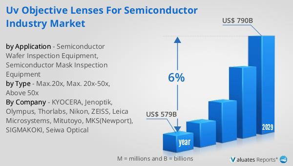
The global semiconductor market was valued at approximately $579 billion in 2022 and is anticipated to reach around $790 billion by 2029, reflecting a compound annual growth rate (CAGR) of 6% over the forecast period. This growth is indicative of the increasing demand for semiconductors, driven by advancements in technology and the proliferation of electronic devices. Semiconductors are the backbone of modern electronics, powering everything from smartphones and computers to advanced medical equipment and automotive systems. The continuous evolution of technology, including the rise of artificial intelligence, the Internet of Things (IoT), and 5G networks, is fueling the demand for more sophisticated and powerful semiconductor devices. As a result, the semiconductor industry is experiencing significant growth, with companies investing heavily in research and development to create more advanced and efficient products. The projected growth of the semiconductor market highlights the importance of innovation and technological advancement in driving the industry forward. As the demand for semiconductors continues to rise, the industry will need to adapt and evolve to meet the changing needs of the market, ensuring that it remains at the forefront of technological progress.
| Report Metric | Details |
| Report Name | UV Objective Lenses for Semiconductor Industry Market |
| Accounted market size in year | US$ 579 billion |
| Forecasted market size in 2029 | US$ 790 billion |
| CAGR | 6% |
| Base Year | year |
| Forecasted years | 2025 - 2029 |
| by Type |
|
| by Application |
|
| Production by Region |
|
| Consumption by Region |
|
| By Company | KYOCERA, Jenoptik, Olympus, Thorlabs, Nikon, ZEISS, Leica Microsystems, Mitutoyo, MKS(Newport), SIGMAKOKI, Seiwa Optical |
| Forecast units | USD million in value |
| Report coverage | Revenue and volume forecast, company share, competitive landscape, growth factors and trends |


