What is Global Automated Wafer Bonder Market?
The Global Automated Wafer Bonder Market is a specialized segment within the semiconductor industry that focuses on the development and sale of machines designed to bond wafers automatically. These machines are crucial in the manufacturing process of semiconductors, as they ensure precise alignment and bonding of wafers, which are thin slices of semiconductor material used in electronics. Automated wafer bonders are essential for producing high-quality, reliable semiconductor devices, as they enhance the efficiency and accuracy of the bonding process. This market is driven by the increasing demand for advanced electronic devices, such as smartphones, tablets, and other consumer electronics, as well as the growing need for miniaturization and higher performance in semiconductor components. The market encompasses various types of wafer bonders, including those designed for different wafer sizes and bonding techniques, catering to the diverse needs of semiconductor manufacturers worldwide.
200 mm, 300 mm in the Global Automated Wafer Bonder Market:
In the Global Automated Wafer Bonder Market, wafer sizes such as 200 mm and 300 mm play a significant role. The 200 mm wafer bonders are widely used in the semiconductor industry due to their cost-effectiveness and compatibility with existing manufacturing infrastructure. These bonders are suitable for producing a wide range of semiconductor devices, including microelectromechanical systems (MEMS), sensors, and power devices. The 200 mm wafer bonders offer a balance between performance and cost, making them an attractive option for many semiconductor manufacturers. On the other hand, 300 mm wafer bonders are gaining popularity due to their ability to produce larger volumes of semiconductor devices with higher efficiency. The larger wafer size allows for more chips to be produced per wafer, reducing the overall cost of production and increasing the throughput. This is particularly important for high-volume applications, such as memory devices and advanced logic chips, where economies of scale are crucial. The 300 mm wafer bonders also offer advanced features, such as higher precision and automation, which further enhance the efficiency and reliability of the bonding process. As the demand for advanced semiconductor devices continues to grow, the adoption of 300 mm wafer bonders is expected to increase, driven by the need for higher performance and cost-effective manufacturing solutions. Both 200 mm and 300 mm wafer bonders are essential components of the Global Automated Wafer Bonder Market, catering to the diverse needs of semiconductor manufacturers and enabling the production of a wide range of electronic devices.
Packaging, MEMS, Others in the Global Automated Wafer Bonder Market:
The Global Automated Wafer Bonder Market finds extensive usage in various applications, including packaging, MEMS, and other areas. In the packaging sector, automated wafer bonders are used to create reliable and high-performance semiconductor packages. These packages protect the semiconductor devices from environmental factors and mechanical damage, ensuring their longevity and functionality. Automated wafer bonders enable precise alignment and bonding of wafers, which is crucial for creating advanced packaging solutions, such as system-in-package (SiP) and wafer-level packaging (WLP). These advanced packaging techniques are essential for producing compact and high-performance electronic devices, such as smartphones, tablets, and wearable devices. In the MEMS sector, automated wafer bonders are used to manufacture microelectromechanical systems, which are tiny devices that combine mechanical and electrical components. MEMS devices are used in a wide range of applications, including sensors, actuators, and microfluidic devices. Automated wafer bonders ensure the precise alignment and bonding of MEMS wafers, which is crucial for the performance and reliability of these devices. The high precision and automation capabilities of wafer bonders enable the production of complex MEMS devices with high yield and consistency. In addition to packaging and MEMS, automated wafer bonders are also used in other areas, such as power devices, photonics, and optoelectronics. These applications require precise and reliable bonding of wafers to ensure the performance and reliability of the final devices. The versatility and advanced features of automated wafer bonders make them an essential tool for semiconductor manufacturers, enabling the production of a wide range of high-performance electronic devices.
Global Automated Wafer Bonder Market Outlook:
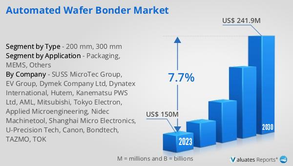
The global Automated Wafer Bonder market was valued at US$ 150 million in 2023 and is anticipated to reach US$ 241.9 million by 2030, witnessing a CAGR of 7.7% during the forecast period from 2024 to 2030. North America, Europe, and Japan collectively hold a market share of 23%. This growth is driven by the increasing demand for advanced semiconductor devices and the need for efficient and reliable manufacturing solutions. The market is characterized by the presence of several key players who are continuously innovating and developing new technologies to meet the evolving needs of the semiconductor industry. The adoption of automated wafer bonders is expected to increase as semiconductor manufacturers seek to enhance their production capabilities and reduce costs. The market outlook remains positive, with significant growth opportunities in various regions and applications. The continuous advancements in wafer bonding technologies and the increasing demand for high-performance electronic devices are expected to drive the growth of the Global Automated Wafer Bonder Market in the coming years.
| Report Metric | Details |
| Report Name | Automated Wafer Bonder Market |
| Accounted market size in 2023 | US$ 150 million |
| Forecasted market size in 2030 | US$ 241.9 million |
| CAGR | 7.7% |
| Base Year | 2023 |
| Forecasted years | 2024 - 2030 |
| Segment by Type |
|
| Segment by Application |
|
| Production by Region |
|
| Consumption by Region |
|
| By Company | SUSS MicroTec Group, EV Group, Dymek Company Ltd, Dynatex International, Hutem, Kanematsu PWS Ltd, AML, Mitsubishi, Tokyo Electron, Applied Microengineering, Nidec Machinetool, Shanghai Micro Electronics, U-Precision Tech, Canon, Bondtech, TAZMO, TOK |
| Forecast units | USD million in value |
| Report coverage | Revenue and volume forecast, company share, competitive landscape, growth factors and trends |


