What is Global Wafer Processing Transport Carriers Market?
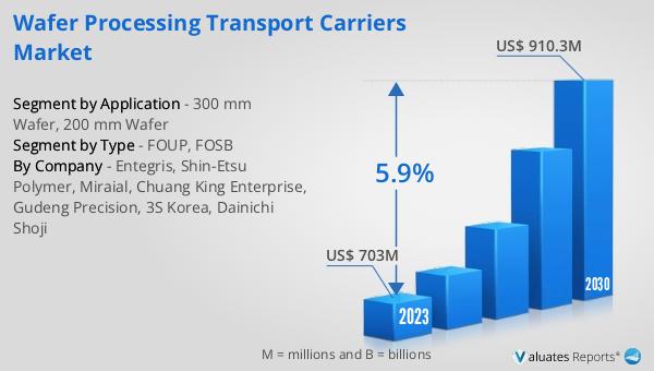
The Global Wafer Processing Transport Carriers Market is a specialized segment within the semiconductor industry, focusing on the devices and containers used for the safe and efficient transport of silicon wafers during the manufacturing process. These carriers are essential for protecting the wafers from contamination and damage as they move through various stages of production, from slicing and polishing to circuit patterning. The market's significance stems from the critical role that silicon wafers play as the foundational material for semiconductor devices. As the demand for semiconductors continues to surge, driven by advancements in technology and the proliferation of electronic devices, the need for reliable wafer transport solutions becomes increasingly paramount. This market caters to a wide range of wafer sizes, but most notably includes carriers designed for the industry-standard 300 mm and 200 mm wafers. The value of the Global Wafer Processing Transport Carriers Market was pegged at approximately 703 million USD in 2023, with projections suggesting growth to around 910.3 million USD by 2030, reflecting a compound annual growth rate (CAGR) of 5.9% over the forecast period. This growth trajectory underscores the market's vital role in supporting the semiconductor industry's expansion and the ongoing innovation within the field of electronics manufacturing.
FOUP, FOSB in the Global Wafer Processing Transport Carriers Market:
FOUP (Front Opening Unified Pod) and FOSB (Front Opening Shipping Box) are integral components of the Global Wafer Processing Transport Carriers Market, serving as advanced solutions for the handling and transportation of silicon wafers in cleanroom environments. FOUPs are specifically designed to hold 300 mm wafers, providing a secure and contaminant-free environment for the wafers as they are transported between various processing steps in the semiconductor manufacturing process. These carriers are constructed from materials that minimize particle generation, such as polycarbonate or polypropylene, and are equipped with a specially designed seal to prevent contamination. FOSBs, on the other hand, are used for both 200 mm and 300 mm wafers and are primarily utilized for the shipping of wafers between manufacturing facilities. They are designed to offer robust protection against physical damage and contamination during transportation. The significance of FOUPs and FOSBs in the Global Wafer Processing Transport Carriers Market cannot be overstated, as they directly impact the efficiency and yield of semiconductor manufacturing processes. The adoption of these carriers is driven by the need for stringent contamination control measures, given the sensitivity of wafers to impurities and the high cost associated with wafer damage. As the semiconductor industry continues to evolve towards more complex and miniaturized devices, the demand for sophisticated wafer transport solutions like FOUPs and FOSBs is expected to grow, further propelling the market's expansion.
300 mm Wafer, 200 mm Wafer in the Global Wafer Processing Transport Carriers Market:
In the realm of semiconductor manufacturing, the Global Wafer Processing Transport Carriers Market plays a pivotal role, especially in the context of 300 mm and 200 mm wafers. These two wafer sizes are among the most commonly used in the industry, with 300 mm wafers being the standard for modern semiconductor fabrication due to their efficiency and higher yield per wafer. The transport carriers designed for these wafers are critical for ensuring the safe handling and contamination-free transfer of wafers through the various stages of production. For 300 mm wafers, the carriers are typically more sophisticated, reflecting the higher value of the wafers and the more stringent requirements of advanced semiconductor processes. These carriers ensure that the wafers are securely housed and protected from any potential contaminants, which is crucial for maintaining the integrity of the manufacturing process and maximizing yield. On the other hand, 200 mm wafer carriers, while also designed to protect the wafers from contamination and damage, cater to processes and facilities that may not require the same level of sophistication as those dealing with 300 mm wafers. Despite these differences, the importance of reliable transport carriers for both wafer sizes cannot be understated, as they are essential for the efficient and cost-effective production of semiconductor devices. The Global Wafer Processing Transport Carriers Market's focus on catering to these needs underscores its critical role in supporting the semiconductor industry's ongoing growth and technological advancement.
Global Wafer Processing Transport Carriers Market Outlook:
The market outlook for the Global Wafer Processing Transport Carriers Market reveals a promising growth trajectory, with the market's valuation starting at 703 million USD in 2023 and expected to climb to 910.3 million USD by 2030. This growth, representing a compound annual growth rate (CAGR) of 5.9% during the forecast period from 2024 to 2030, highlights the increasing demand for wafer processing transport carriers. Taiwan emerges as the leading consumer within this market, accounting for nearly 19.75% of the global consumption share in 2022, which underscores the region's pivotal role in the semiconductor manufacturing industry. Furthermore, the market is characterized by a high concentration of market share among the top five companies globally, which collectively hold 96.32% of the market. This concentration indicates a competitive landscape where these leading companies play a crucial role in shaping market dynamics, innovation, and the development of new and improved wafer transport solutions. The market's growth is fueled by the expanding semiconductor industry, which relies heavily on the efficient and safe transportation of wafers, making the role of transport carriers indispensable for the production of high-quality semiconductor devices.
| Report Metric | Details |
| Report Name | Wafer Processing Transport Carriers Market |
| Accounted market size in 2023 | US$ 703 million |
| Forecasted market size in 2030 | US$ 910.3 million |
| CAGR | 5.9% |
| Base Year | 2023 |
| Forecasted years | 2024 - 2030 |
| Segment by Type |
|
| Segment by Application |
|
| Production by Region |
|
| Consumption by Region |
|
| By Company | Entegris, Shin-Etsu Polymer, Miraial, Chuang King Enterprise, Gudeng Precision, 3S Korea, Dainichi Shoji |
| Forecast units | USD million in value |
| Report coverage | Revenue and volume forecast, company share, competitive landscape, growth factors and trends |


