What is Global Semiconductor Wet Etching Equipment Market?
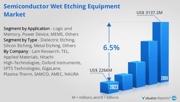
The Global Semiconductor Wet Etching Equipment Market is a specialized segment within the semiconductor manufacturing industry, focusing on the use of wet chemical processes to etch away parts of semiconductor wafers in order to create the desired circuit patterns. This market is crucial for the production of various electronic devices, as it directly impacts the efficiency, performance, and miniaturization of semiconductor components. Wet etching equipment utilizes liquid chemicals or etchants to remove material from the semiconductor substrate. This process is essential for the fabrication of integrated circuits and various semiconductor devices. The market's significance stems from its role in enabling the production of highly precise and complex microstructures, which are fundamental to the modern electronics industry. As of 2023, the market has been valued at approximately US$ 2266 million, with projections suggesting a growth to US$ 3137.2 million by 2030. This growth is attributed to the continuous advancements in semiconductor technology, increasing demand for electronic devices, and the expansion of semiconductor manufacturing capabilities worldwide. The market's expansion reflects the ongoing innovation and technological progress within the semiconductor industry, highlighting the critical role of wet etching equipment in meeting the evolving demands for more sophisticated electronic components.
Dielectric Etching, Silicon Etching, Metal Etching, Others in the Global Semiconductor Wet Etching Equipment Market:
Dielectric Etching, Silicon Etching, Metal Etching, and others are key processes within the Global Semiconductor Wet Etching Equipment Market, each serving a unique purpose in semiconductor fabrication. Dielectric etching is used to shape insulating materials on a chip, crucial for creating the multilayer structures that modern integrated circuits require. This process ensures that electrical components within a chip are properly isolated, enhancing the device's performance and reliability. Silicon etching, on the other hand, is fundamental for shaping the silicon substrate itself, creating the wells and trenches needed for the transistors that form the heart of digital circuits. Metal etching is employed to pattern the metal layers that connect the various components on a chip, enabling the complex interconnections that define a circuit's functionality. Each of these etching processes requires precise control over the chemical reactions involved to ensure the high fidelity of the resulting structures, with the choice of etchant and process parameters tailored to the specific material being etched. Beyond these, the category of 'others' encompasses a range of specialized etching processes, including those for advanced materials and novel fabrication techniques that are continually being developed to push the boundaries of semiconductor technology. The diversity and complexity of these etching processes underscore the critical role of wet etching equipment in enabling the production of increasingly sophisticated semiconductor devices, driving the market's growth as the industry evolves toward ever-smaller, faster, and more efficient electronic components.
Logic and Memory, Power Device, MEMS, Others in the Global Semiconductor Wet Etching Equipment Market:
The usage of Global Semiconductor Wet Etching Equipment Market spans across various areas such as Logic and Memory, Power Device, MEMS, and others, each playing a pivotal role in the semiconductor industry. In Logic and Memory, wet etching equipment is indispensable for the fabrication of the intricate circuits that form the backbone of computing devices, from smartphones to servers. This area relies on the precision and control offered by wet etching to create the complex patterns required for advanced logic circuits and high-density memory arrays. For Power Devices, which are essential for managing power in electronic systems, wet etching processes are used to create the structures that ensure efficient power conversion and distribution, contributing to the overall performance and reliability of electronic devices. MEMS, or Micro-Electro-Mechanical Systems, benefit from the delicate and precise etching capabilities of wet etching equipment to fabricate the tiny mechanical and electrical components that enable sensors, actuators, and other microdevices. The 'others' category encompasses a broad range of applications, including but not limited to, photonics, bioelectronics, and advanced packaging technologies, each requiring the specific capabilities of wet etching processes to realize the unique structures and functionalities demanded by these cutting-edge applications. The versatility and adaptability of wet etching equipment to meet the needs of these diverse areas underscore its critical importance in the semiconductor manufacturing ecosystem, driving innovation and enabling the continued miniaturization and performance enhancement of electronic devices.
Global Semiconductor Wet Etching Equipment Market Outlook:
The market outlook for the Global Semiconductor Wet Etching Equipment Market reveals a promising trajectory, with the market's value standing at US$ 2266 million in 2023 and projected to ascend to US$ 3137.2 million by 2030, marking a Compound Annual Growth Rate (CAGR) of 6.5% throughout the forecast period spanning from 2024 to 2030. This growth is indicative of the robust demand and ongoing advancements within the semiconductor industry, reflecting the critical role of wet etching equipment in the fabrication of semiconductor devices. The market's expansion is further underscored by the significant market share held by regions such as North America, Europe, and Japan, which together account for 23% of the global market. This distribution highlights the strategic importance of these regions in the semiconductor manufacturing landscape, driven by their technological leadership and the presence of key industry players. The projected growth and regional market shares underscore the dynamic nature of the semiconductor wet etching equipment market, reflecting both the technological advancements driving the industry forward and the strategic investments being made across key regions to bolster their semiconductor manufacturing capabilities.
| Report Metric | Details |
| Report Name | Semiconductor Wet Etching Equipment Market |
| Accounted market size in 2023 | US$ 2266 million |
| Forecasted market size in 2030 | US$ 3137.2 million |
| CAGR | 6.5% |
| Base Year | 2023 |
| Forecasted years | 2024 - 2030 |
| Segment by Type |
|
| Segment by Application |
|
| Production by Region |
|
| Consumption by Region |
|
| By Company | Lam Research, TEL, Applied Materials, Hitachi High-Technologies, Oxford Instruments, SPTS Technologies, GigaLane, Plasma-Therm, SAMCO, AMEC, NAURA |
| Forecast units | USD million in value |
| Report coverage | Revenue and volume forecast, company share, competitive landscape, growth factors and trends |