What is Global Semiconductor Wafer Transfer Robotics Market?
The Global Semiconductor Wafer Transfer Robotics Market is a specialized sector within the broader semiconductor industry, focusing on the development, manufacturing, and sale of robotic systems designed for the handling and transfer of semiconductor wafers. These robotic systems are crucial for the semiconductor manufacturing process, ensuring the precise and clean movement of wafers through various stages of production without contaminating or damaging them. As semiconductors are the backbone of modern electronics, including smartphones, computers, and countless other devices, the demand for more efficient and advanced wafer transfer robotics has surged. This market encompasses a range of robotic technologies, including vacuum and edge grip systems, designed to accommodate different sizes and types of wafers. With the semiconductor industry pushing towards smaller, more powerful devices, the role of wafer transfer robotics becomes increasingly critical, driving innovation and efficiency in semiconductor manufacturing processes. The market's growth is propelled by the continuous expansion of the semiconductor industry, technological advancements in robotics, and the increasing complexity of semiconductor device fabrication, which requires more sophisticated handling solutions to maintain high yields and production standards.
300 mm Wafer, 200 mm Wafer, Others in the Global Semiconductor Wafer Transfer Robotics Market:
In the realm of the Global Semiconductor Wafer Transfer Robotics Market, the categorization based on wafer sizes, such as 300 mm, 200 mm, and others, plays a pivotal role in understanding market dynamics. The 300 mm wafer segment represents the forefront of semiconductor manufacturing, offering economies of scale that significantly reduce the cost per chip. Robotics systems designed for handling these wafers are equipped with advanced technologies to manage the increased size and weight, ensuring precise and safe transfer during the production process. On the other hand, the 200 mm wafer segment, while older, remains relevant due to its widespread use in numerous applications and the existence of established production facilities specifically designed for this size. Robotics systems for 200 mm wafers are tailored to operate within these legacy environments, providing upgrades and maintenance to extend the life of existing lines. The "others" category encompasses robotics solutions for emerging and niche applications, including but not limited to, smaller wafer sizes used in specific types of semiconductor devices or research and development settings. This diversity in wafer sizes necessitates a broad range of robotic systems, each optimized for specific handling requirements, to ensure the semiconductor manufacturing process remains efficient, cost-effective, and capable of meeting the evolving demands of the industry. The development and refinement of these robotic systems are driven by the continuous push for miniaturization, higher performance, and lower costs in semiconductor devices, making the wafer size-based segmentation a critical aspect of market analysis and product development strategies in the global semiconductor wafer transfer robotics market.
IDM, Foundry in the Global Semiconductor Wafer Transfer Robotics Market:
In the Global Semiconductor Wafer Transfer Robotics Market, the usage of robotics in Integrated Device Manufacturers (IDM) and Foundries showcases the diverse applications and benefits of these systems in the semiconductor manufacturing ecosystem. IDMs, companies that design, manufacture, and sell their semiconductor products, utilize wafer transfer robotics to streamline their in-house production processes. These robots play a crucial role in maintaining the cleanliness and integrity of wafers as they move through various stages of fabrication, from lithography to packaging. The precision and reliability of robotics help IDMs achieve higher yields, reduce production costs, and accelerate time-to-market for their products. In contrast, Foundries, which are specialized facilities that manufacture chips on behalf of other companies, leverage wafer transfer robotics to offer flexible and efficient manufacturing solutions. Given the foundries' need to accommodate a wide range of customer requirements and rapidly switch between different production runs, robotics systems provide the agility and scalability necessary to manage diverse and complex processes. The use of robotics in both IDMs and Foundries underscores the critical role of automation in enhancing productivity, ensuring product quality, and supporting the dynamic needs of the semiconductor industry. As the demand for semiconductors continues to grow, driven by advancements in technology and the proliferation of electronic devices, the reliance on wafer transfer robotics in IDMs and Foundries is set to increase, further propelling the growth and evolution of the Global Semiconductor Wafer Transfer Robotics Market.
Global Semiconductor Wafer Transfer Robotics Market Outlook:
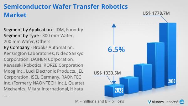
The market outlook for the Global Semiconductor Wafer Transfer Robotics sector presents a promising future, with the market's value estimated at US$ 1333.5 million in 2023, and projections suggest it will ascend to US$ 1778.7 million by 2030. This growth trajectory, characterized by a compound annual growth rate (CAGR) of 6.5% during the forecast period from 2024 to 2030, underscores the increasing reliance on and demand for semiconductor wafer transfer robotics across the industry. The significance of this market is further highlighted by the substantial market share held by North America, Europe, and Japan, which collectively account for 23% of the global market. This data points to the strategic importance of these regions in the development, innovation, and adoption of wafer transfer robotics technologies. The anticipated expansion of the market is driven by several factors, including the continuous advancement in semiconductor technology, the growing complexity of semiconductor device manufacturing processes, and the increasing need for efficiency and precision in wafer handling. As the semiconductor industry moves towards more sophisticated and miniaturized devices, the role of robotics in ensuring the seamless transfer of wafers through the production line becomes ever more critical, setting the stage for sustained growth and innovation in the Global Semiconductor Wafer Transfer Robotics Market.
| Report Metric | Details |
| Report Name | Semiconductor Wafer Transfer Robotics Market |
| Accounted market size in 2023 | US$ 1333.5 million |
| Forecasted market size in 2030 | US$ 1778.7 million |
| CAGR | 6.5% |
| Base Year | 2023 |
| Forecasted years | 2024 - 2030 |
| Segment by Type |
|
| Segment by Application |
|
| Production by Region |
|
| Consumption by Region |
|
| By Company | Brooks Automation, Kensington Laboratories, Nidec Sankyo Corporation, DAIHEN Corporation, Kawasaki Robotics, RORZE Corporation, Moog Inc., Ludl Electronic Products, JEL Corporation, ISEL Germany, RAONTEC Inc. (Formerly NAONTECH Inc.), Quartet Mechanics, Milara International, Hirata Corporation, MEIKIKOU Corporation, SINFONIA TECHNOLOGY, KORO, YASKAWA |
| Forecast units | USD million in value |
| Report coverage | Revenue and volume forecast, company share, competitive landscape, growth factors and trends |