What is Global Semiconductor Wafer Polishing Pad Market?
The Global Semiconductor Wafer Polishing Pad Market is a specialized segment within the semiconductor industry, focusing on the production and distribution of polishing pads used in the manufacturing of semiconductor wafers. These polishing pads are crucial components in the semiconductor fabrication process, particularly in the planarization step, which smoothens the silicon wafer's surface to prepare it for intricate circuit patterning. The market's significance stems from the relentless pursuit of miniaturization and performance enhancement in electronic devices, driving the demand for ever-more precise and efficient polishing technologies. As semiconductor devices become smaller and more complex, the role of the polishing pad in ensuring the production of high-quality wafers becomes increasingly critical. The market encompasses a variety of pad types, each designed to meet specific requirements of the wafer polishing process, including material composition, pad hardness, and surface texture. With the semiconductor industry's growth, driven by expanding applications in consumer electronics, automotive, and industrial automation, the demand for semiconductor wafer polishing pads is expected to rise, reflecting the sector's vital role in the global technology landscape.
Hard Pad, Soft Pad in the Global Semiconductor Wafer Polishing Pad Market:
In the realm of the Global Semiconductor Wafer Polishing Pad Market, two primary categories of polishing pads play pivotal roles: Hard Pads and Soft Pads. Hard pads are typically made from materials that offer higher rigidity and are used in the initial stages of the polishing process to remove major surface irregularities and topography variations. These pads are essential for ensuring that the wafer surface is uniformly flat before finer polishing steps. On the other hand, soft pads, crafted from more pliable materials, are employed in the latter stages of polishing. They are crucial for achieving the ultra-smooth surfaces required for advanced semiconductor devices, as they can conform more closely to the wafer's surface, allowing for the removal of minute imperfections and scratches. The distinction between hard and soft pads is not merely about the material hardness but also involves differences in pad design, including pore structure, compressibility, and surface texture, each of which influences the polishing efficiency and outcome. Manufacturers and researchers continuously innovate in the composition and structure of these pads to enhance their performance, reduce defect rates, and meet the increasingly stringent requirements of semiconductor fabrication. As the semiconductor industry pushes towards smaller feature sizes and more complex architectures, the role of both hard and soft polishing pads becomes ever more critical, with ongoing developments aimed at optimizing the balance between material removal efficiency and surface finish quality.
300 mm Wafer, 200 mm Wafer, Others in the Global Semiconductor Wafer Polishing Pad Market:
The usage of the Global Semiconductor Wafer Polishing Pad Market spans across various wafer sizes, notably including 300 mm wafers, 200 mm wafers, and others. The 300 mm wafer segment represents the forefront of semiconductor manufacturing, offering economies of scale and higher throughput for chipmakers. Polishing pads designed for these wafers are engineered to meet the demands of high-volume production while maintaining the precision required for advanced semiconductor devices. The uniformity and surface finish achieved in the polishing process are critical for ensuring the performance and yield of chips produced on these larger wafers. Meanwhile, the 200 mm wafer segment, although older, remains relevant in the production of a wide range of semiconductor devices. Polishing pads for 200 mm wafers continue to be optimized for various applications, balancing cost and performance for technologies that do not require the cutting-edge features of the latest node sizes. The "others" category encompasses emerging and specialized applications, including smaller wafer sizes and non-standard substrates, which require customized polishing solutions. These diverse applications highlight the versatility and adaptability of polishing pad technologies to meet the needs of different segments of the semiconductor market. As the industry evolves, the development of polishing pads will continue to play a crucial role in enabling the production of high-quality wafers across all segments, reflecting the dynamic nature of semiconductor manufacturing and the continuous push for innovation.
Global Semiconductor Wafer Polishing Pad Market Outlook:
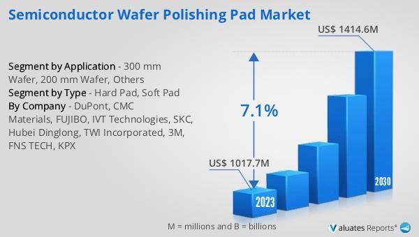
The market outlook for the Global Semiconductor Wafer Polishing Pad Market presents a promising future, with its valuation at approximately 1017.7 million US dollars as of 2023. This figure is projected to ascend to around 1414.6 million US dollars by the year 2030, marking a Compound Annual Growth Rate (CAGR) of 7.1% throughout the forecast period spanning from 2024 to 2030. This anticipated growth underscores the increasing importance and demand for semiconductor wafer polishing pads in the semiconductor manufacturing process. As the industry continues to advance, driven by the relentless demand for more powerful and efficient electronic devices, the need for high-quality polishing pads that can meet the stringent requirements of modern semiconductor fabrication processes becomes ever more critical. This growth trajectory reflects the broader trends in the semiconductor industry, including the push towards smaller device geometries and the expansion of semiconductor applications across various sectors. The market's robust growth prospects highlight the pivotal role that semiconductor wafer polishing pads play in enabling the production of the next generation of semiconductor devices.
| Report Metric | Details |
| Report Name | Semiconductor Wafer Polishing Pad Market |
| Accounted market size in 2023 | US$ 1017.7 million |
| Forecasted market size in 2030 | US$ 1414.6 million |
| CAGR | 7.1% |
| Base Year | 2023 |
| Forecasted years | 2024 - 2030 |
| Segment by Type |
|
| Segment by Application |
|
| Production by Region |
|
| Consumption by Region |
|
| By Company | DuPont, CMC Materials, FUJIBO, IVT Technologies, SKC, Hubei Dinglong, TWI Incorporated, 3M, FNS TECH, KPX |
| Forecast units | USD million in value |
| Report coverage | Revenue and volume forecast, company share, competitive landscape, growth factors and trends |


