What is Global Photomask for Semiconductor Market?
The Global Photomask for Semiconductor Market is a critical segment within the semiconductor industry, focusing on the production and supply of photomasks, which are essential tools in the fabrication of semiconductors. Photomasks are used to transfer circuit patterns onto semiconductor wafers during the lithography process in semiconductor manufacturing, acting as a blueprint for the microcircuit designs. These masks are meticulously crafted to ensure high precision and accuracy, as they directly influence the performance and yield of semiconductor devices. The market's significance stems from the relentless demand for more advanced and miniaturized semiconductor components, driven by the continuous evolution of electronic devices. As technologies advance, the complexity and requirements for photomasks increase, pushing the market towards innovative solutions to meet the stringent specifications of next-generation semiconductor devices. The market encompasses a range of photomask types, including those used for extreme ultraviolet (EUV) lithography, deep ultraviolet (DUV) lithography, and traditional optical lithography, each catering to different segments of semiconductor manufacturing. The demand for photomasks is closely tied to the semiconductor industry's growth trajectory, with trends such as the expansion of 5G technology, artificial intelligence, and the Internet of Things (IoT) further fueling the need for sophisticated semiconductor components and, by extension, for high-quality photomasks.
EUV Mask, UV and DUV Mask in the Global Photomask for Semiconductor Market:
In the realm of the Global Photomask for Semiconductor Market, EUV Mask, UV, and DUV Mask stand out as pivotal components in the semiconductor manufacturing process, each serving distinct roles based on the lithography techniques they are associated with. EUV masks, designed for extreme ultraviolet lithography, represent the cutting edge in photomask technology, catering to the fabrication of semiconductor devices with incredibly fine features, down to the 7nm node and beyond. These masks are crucial for producing high-density integrated circuits found in advanced computing and mobile devices, leveraging shorter wavelength light to achieve unparalleled precision. On the other hand, DUV masks are tailored for deep ultraviolet lithography, a technique that, while not as advanced as EUV, is instrumental in manufacturing semiconductors with feature sizes ranging from 10nm to 250nm. DUV lithography remains a workhorse in the industry, suitable for a wide array of applications that do not require the extreme miniaturization offered by EUV. UV masks, utilized in traditional ultraviolet lithography, cater to even larger feature sizes and are pivotal in the production of a variety of semiconductor devices that demand less stringent resolution requirements. The differentiation between these masks underscores the semiconductor industry's layered approach to device fabrication, where different technologies coexist and are selected based on the specific needs of the semiconductor devices being produced. As the industry pushes towards more compact and efficient devices, the role of these masks, especially EUV masks, becomes increasingly critical, highlighting the ongoing advancements in photomask technology and its direct impact on the capabilities and performance of semiconductor components.
IC Manufacturing, IC Packaging in the Global Photomask for Semiconductor Market:
The usage of the Global Photomask for Semiconductor Market in areas such as IC Manufacturing and IC Packaging is a testament to the indispensable role photomasks play in the semiconductor production ecosystem. In IC Manufacturing, photomasks are the cornerstone of the lithography process, where they serve as the master templates for transferring circuit patterns onto semiconductor wafers. This process is repeated multiple times, with different masks used at various stages of the manufacturing to build up the complex layers of an integrated circuit. The precision and quality of these photomasks directly influence the fidelity of the pattern transfer, impacting the performance, yield, and reliability of the final semiconductor products. As devices become more sophisticated, requiring smaller feature sizes and more complex circuitry, the demand for high-resolution photomasks escalates, pushing the boundaries of photomask technology. In the realm of IC Packaging, photomasks also play a crucial role, albeit in a different context. They are used in the fabrication of the package substrates and in the lithography steps involved in advanced packaging techniques, such as flip-chip or through-silicon via (TSV) technologies. These packaging processes require photomasks to create the intricate patterns needed for the connections between the semiconductor die and the package, as well as between the package and the external environment. The precision of these patterns is vital for ensuring the electrical performance and reliability of the packaged semiconductor device, further underscoring the importance of photomasks in the broader semiconductor manufacturing process. As the industry continues to evolve towards more complex IC designs and packaging solutions, the role of photomasks in enabling these advancements remains unequivocally central.
Global Photomask for Semiconductor Market Outlook:
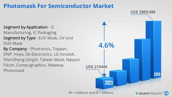
The market outlook for the Global Photomask for Semiconductor Market and the broader semiconductor industry presents a promising growth trajectory in the coming years. In 2023, the photomask market was valued at approximately $2104 million, with projections suggesting an increase to around $2869.8 million by 2030, reflecting a compound annual growth rate (CAGR) of 4.6% over the forecast period from 2024 to 2030. This growth is indicative of the vital role photomasks play in semiconductor manufacturing, driven by the industry's relentless pursuit of miniaturization and performance enhancement. Concurrently, the semiconductor market itself, valued at $579 billion in 2022, is on a path to reach $790 billion by 2029, growing at a CAGR of 6% during the forecast period. This expansion is fueled by the increasing demand for semiconductor devices across a wide range of applications, from consumer electronics and automotive to industrial automation and telecommunications, particularly with the advent of 5G technology, artificial intelligence, and the Internet of Things (IoT). The intertwined growth of the photomask and semiconductor markets underscores the symbiotic relationship between the demand for advanced semiconductor devices and the need for high-precision photomasks required for their production. As the semiconductor industry continues to innovate and expand, the photomask market is poised to play an increasingly critical role in enabling the next generation of semiconductor technologies.
| Report Metric | Details |
| Report Name | Photomask for Semiconductor Market |
| Accounted market size in 2023 | US$ 2104 million |
| Forecasted market size in 2030 | US$ 2869.8 million |
| CAGR | 4.6% |
| Base Year | 2023 |
| Forecasted years | 2024 - 2030 |
| Segment by Type |
|
| Segment by Application |
|
| Production by Region |
|
| Consumption by Region |
|
| By Company | Photronics, Toppan, DNP, Hoya, SK-Electronics, LG Innotek, ShenZheng QingVi, Taiwan Mask, Nippon Filcon, Compugraphics, Newway Photomask |
| Forecast units | USD million in value |
| Report coverage | Revenue and volume forecast, company share, competitive landscape, growth factors and trends |


