What is Global Gallium Nitride RF Semiconductor Device Market?
The Global Gallium Nitride (GaN) RF Semiconductor Device Market is a rapidly evolving sector within the broader semiconductor industry. Gallium Nitride is a material that offers significant advantages over traditional silicon-based semiconductors, particularly in high-frequency and high-power applications. These devices are crucial in various applications, including telecommunications, military, and aerospace, due to their ability to operate at higher voltages, frequencies, and temperatures. The market for GaN RF semiconductors is driven by the increasing demand for efficient and compact power conversion systems, as well as the growing need for advanced communication systems. The technology's ability to enhance performance while reducing energy consumption makes it highly attractive for industries looking to improve efficiency and reduce costs. As a result, the GaN RF semiconductor market is experiencing significant growth, with numerous companies investing in research and development to capitalize on the potential of this technology. The market's expansion is further supported by the increasing adoption of 5G technology, which requires high-performance RF components to meet the demands of faster and more reliable communication networks. Overall, the Global GaN RF Semiconductor Device Market is poised for continued growth as industries seek to leverage its benefits for various applications.
2 Inch, 4 Inch, 6-Inch and Above in the Global Gallium Nitride RF Semiconductor Device Market:
In the Global Gallium Nitride RF Semiconductor Device Market, wafer sizes such as 2-inch, 4-inch, 6-inch, and above play a crucial role in determining the production capacity and cost-effectiveness of semiconductor devices. The 2-inch wafers are typically used in research and development settings or for niche applications where smaller quantities of GaN devices are required. These wafers are often employed in experimental setups to test new designs and materials before scaling up to larger wafer sizes. Despite their limited production capacity, 2-inch wafers are essential for innovation and the development of next-generation GaN technologies. Moving to 4-inch wafers, these are more commonly used in small to medium-scale production environments. They offer a balance between production efficiency and cost, making them suitable for a variety of applications, including telecommunications and consumer electronics. The 4-inch wafers allow manufacturers to produce a higher volume of devices compared to 2-inch wafers, while still maintaining a relatively low production cost. This makes them an attractive option for companies looking to enter the GaN RF semiconductor market without the need for large-scale production facilities. The 6-inch and above wafers represent the next step in scaling up production capacity. These larger wafers are used in high-volume manufacturing environments where cost efficiency and production throughput are critical. The use of 6-inch and larger wafers allows manufacturers to produce a significantly higher number of devices per wafer, reducing the overall cost per device. This is particularly important in industries such as telecommunications and automotive, where large quantities of GaN devices are required to meet the growing demand for high-performance RF components. The transition to larger wafer sizes is driven by the need to reduce production costs and increase the availability of GaN devices in the market. As the demand for GaN RF semiconductors continues to grow, manufacturers are investing in the development of larger wafer sizes to meet the needs of various industries. The ability to produce GaN devices on larger wafers not only improves production efficiency but also enables manufacturers to offer more competitive pricing, further driving the adoption of GaN technology across different sectors. In summary, the choice of wafer size in the Global Gallium Nitride RF Semiconductor Device Market is a critical factor that influences production capacity, cost, and the overall competitiveness of GaN devices. As the market continues to expand, the trend towards larger wafer sizes is expected to continue, enabling manufacturers to meet the increasing demand for high-performance RF components in a cost-effective manner.
Power Drivers, Supply and Inverter, Radio Frequency, Lighting and Laser in the Global Gallium Nitride RF Semiconductor Device Market:
The Global Gallium Nitride RF Semiconductor Device Market finds its applications in various areas, including power drivers, supply and inverter, radio frequency, lighting, and laser technologies. In power drivers, GaN devices are highly valued for their ability to handle high voltages and currents with greater efficiency than traditional silicon-based devices. This makes them ideal for use in power conversion systems, where efficiency and compactness are critical. GaN power drivers are used in a wide range of applications, from consumer electronics to industrial equipment, where they help reduce energy consumption and improve overall system performance. In supply and inverter applications, GaN semiconductors are used to convert and manage electrical power more efficiently. Their high-frequency operation and low power loss make them suitable for use in renewable energy systems, such as solar inverters and wind turbines, where maximizing energy conversion efficiency is essential. GaN-based inverters are also used in electric vehicles, where they contribute to extending the driving range by improving the efficiency of the powertrain. In the radio frequency domain, GaN RF semiconductors are used in communication systems, radar, and satellite applications. Their ability to operate at high frequencies and power levels makes them ideal for use in 5G networks, where they help improve signal strength and data transmission rates. GaN RF devices are also used in military and aerospace applications, where their robustness and reliability are critical for mission-critical communication systems. In lighting applications, GaN semiconductors are used in LED technology, where they offer improved efficiency and brightness compared to traditional lighting solutions. GaN-based LEDs are used in a variety of applications, from residential and commercial lighting to automotive and display technologies. Their long lifespan and low energy consumption make them an attractive option for reducing energy costs and environmental impact. Finally, in laser applications, GaN semiconductors are used to produce high-power and high-efficiency laser diodes. These lasers are used in a range of applications, from industrial cutting and welding to medical and scientific research. GaN-based lasers offer superior performance and reliability compared to traditional laser technologies, making them a preferred choice for demanding applications. Overall, the Global Gallium Nitride RF Semiconductor Device Market plays a vital role in advancing technology across various sectors, offering improved performance, efficiency, and reliability in a wide range of applications.
Global Gallium Nitride RF Semiconductor Device Market Outlook:
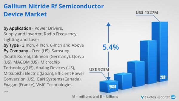
The worldwide market for Gallium Nitride RF Semiconductor Devices was valued at approximately $923 million in 2024. It is anticipated to grow to a revised size of about $1,327 million by 2031, reflecting a compound annual growth rate (CAGR) of 5.4% over the forecast period. This growth is indicative of the increasing demand for GaN RF semiconductors across various industries, driven by their superior performance characteristics compared to traditional silicon-based devices. The broader semiconductor market was estimated to be worth $579 billion in 2022 and is projected to reach $790 billion by 2029, growing at a CAGR of 6% during the forecast period. This growth in the semiconductor market underscores the expanding role of advanced materials like Gallium Nitride in meeting the evolving needs of modern technology. The increasing adoption of 5G technology, the rise of electric vehicles, and the growing demand for energy-efficient solutions are some of the key factors contributing to the growth of the GaN RF semiconductor market. As industries continue to seek ways to enhance performance and reduce energy consumption, the demand for GaN RF semiconductors is expected to rise, further driving the market's expansion. The ongoing investment in research and development by key players in the industry is also expected to contribute to the market's growth, as new and improved GaN technologies are developed to meet the needs of various applications.
| Report Metric | Details |
| Report Name | Gallium Nitride RF Semiconductor Device Market |
| Accounted market size in year | US$ 923 million |
| Forecasted market size in 2031 | US$ 1327 million |
| CAGR | 5.4% |
| Base Year | year |
| Forecasted years | 2025 - 2031 |
| by Type |
|
| by Application |
|
| Production by Region |
|
| Consumption by Region |
|
| By Company | Cree (US), Samsung (South Korea), Infineon (Germany), Qorvo (US), MACOM (US), Microchip Technology(US), Analog Devices (US), Mitsubishi Electric (Japan), Efficient Power Conversion (US), GaN Systems (Canada), Exagan (France), VisIC Technologies (Israel), Integra Technologies (US), Transphorm (US), Navitas Semiconductor (US), Nichia (Japan), Panasonic (Japan), Texas Instruments (US) |
| Forecast units | USD million in value |
| Report coverage | Revenue and volume forecast, company share, competitive landscape, growth factors and trends |


