What is Global Epitaxial Silicon Wafer Market?
The Global Epitaxial Silicon Wafer Market is a crucial segment within the semiconductor industry, playing a vital role in the production of high-performance electronic devices. Epitaxial silicon wafers are specialized substrates used in the fabrication of integrated circuits and other semiconductor devices. These wafers are created through a process called epitaxy, where a thin layer of silicon is deposited onto a crystalline silicon substrate. This process enhances the electrical properties of the wafer, making it suitable for advanced applications in electronics. The demand for epitaxial silicon wafers is driven by the growing need for efficient and high-speed electronic devices, including smartphones, computers, and automotive electronics. As technology continues to advance, the market for these wafers is expected to expand, driven by innovations in semiconductor manufacturing and the increasing adoption of smart technologies across various industries. The global epitaxial silicon wafer market is characterized by continuous research and development efforts aimed at improving wafer quality and reducing production costs, ensuring that it remains a key component in the ever-evolving landscape of modern electronics.
Polished wafer, Epitaxial wafer, Silicon-On-Insulator, Lapping wafer in the Global Epitaxial Silicon Wafer Market:
In the realm of the Global Epitaxial Silicon Wafer Market, several types of wafers play distinct roles, each contributing to the advancement of semiconductor technology. Polished wafers are the most basic form, serving as the foundation for further processing. These wafers undergo a meticulous polishing process to achieve a smooth, mirror-like surface, essential for subsequent layers of semiconductor material. The polished surface ensures minimal defects, which is crucial for the performance and reliability of the final electronic devices. Epitaxial wafers, on the other hand, are a step beyond polished wafers. They involve the deposition of an additional silicon layer on top of the polished wafer. This epitaxial layer is engineered to have specific electrical properties, enhancing the wafer's performance in high-frequency and high-power applications. Epitaxial wafers are particularly valuable in the production of advanced integrated circuits and power devices, where precision and efficiency are paramount. Silicon-On-Insulator (SOI) wafers represent another significant advancement in wafer technology. These wafers consist of a thin layer of silicon separated from the bulk substrate by an insulating layer, typically silicon dioxide. This structure reduces parasitic capacitance, improving the speed and power efficiency of electronic devices. SOI wafers are widely used in the production of microprocessors, RF devices, and sensors, where performance and energy efficiency are critical. Lastly, lapping wafers are an intermediate step in wafer processing, used to achieve the desired thickness and flatness before polishing. The lapping process involves the removal of material from the wafer surface using an abrasive slurry, ensuring uniformity and precision. Each type of wafer, from polished to epitaxial, SOI, and lapping, plays a vital role in the Global Epitaxial Silicon Wafer Market, contributing to the development of cutting-edge semiconductor devices that power modern technology.
Chemical, Medical devices, Industrial in the Global Epitaxial Silicon Wafer Market:
The Global Epitaxial Silicon Wafer Market finds extensive applications across various industries, including chemical, medical devices, and industrial sectors, each leveraging the unique properties of these wafers to enhance their technological capabilities. In the chemical industry, epitaxial silicon wafers are utilized in the production of sensors and detectors that monitor chemical processes. These sensors rely on the precise electrical properties of epitaxial wafers to detect changes in chemical compositions, ensuring accurate and reliable measurements. The high sensitivity and stability of these wafers make them ideal for use in harsh chemical environments, where precision is paramount. In the medical devices sector, epitaxial silicon wafers are integral to the development of advanced diagnostic and therapeutic equipment. Medical imaging devices, such as MRI and CT scanners, benefit from the high-performance capabilities of these wafers, enabling clearer and more detailed images. Additionally, epitaxial wafers are used in the fabrication of microelectromechanical systems (MEMS) for medical applications, including implantable devices and biosensors. The biocompatibility and reliability of these wafers ensure their safe and effective use in medical settings. In the industrial sector, epitaxial silicon wafers are employed in the production of power electronics and control systems. These wafers are essential for the development of efficient power management solutions, enabling the optimization of energy consumption in industrial processes. The robust performance of epitaxial wafers in high-temperature and high-power applications makes them suitable for use in industrial automation, renewable energy systems, and electric vehicles. As industries continue to evolve and demand more sophisticated technologies, the Global Epitaxial Silicon Wafer Market is poised to play a pivotal role in driving innovation and efficiency across these diverse sectors.
Global Epitaxial Silicon Wafer Market Outlook:
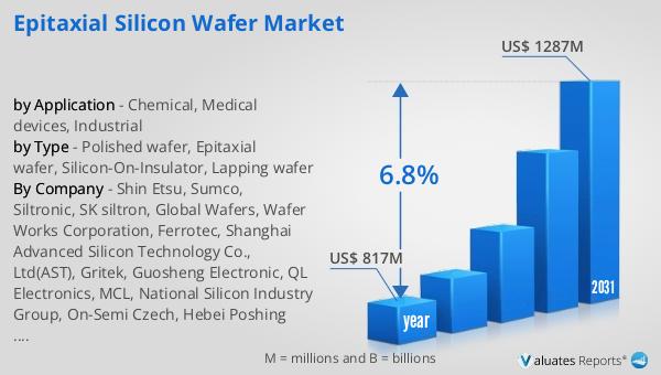
In 2024, the global market for Epitaxial Silicon Wafer was valued at approximately $817 million. Looking ahead, this market is anticipated to grow significantly, reaching an estimated size of $1,287 million by 2031. This growth trajectory represents a compound annual growth rate (CAGR) of 6.8% over the forecast period. The increasing demand for advanced semiconductor devices, driven by technological advancements and the proliferation of smart technologies, is a key factor contributing to this market expansion. As industries across the globe continue to adopt more sophisticated electronic devices, the need for high-quality epitaxial silicon wafers is expected to rise. This growth is further supported by ongoing research and development efforts aimed at enhancing wafer quality and reducing production costs. The market's upward trend reflects the critical role that epitaxial silicon wafers play in the semiconductor industry, serving as a foundation for the development of cutting-edge technologies that power modern electronics. As the market continues to evolve, it is poised to meet the growing demands of various industries, ensuring its relevance and importance in the global technological landscape.
| Report Metric | Details |
| Report Name | Epitaxial Silicon Wafer Market |
| Accounted market size in year | US$ 817 million |
| Forecasted market size in 2031 | US$ 1287 million |
| CAGR | 6.8% |
| Base Year | year |
| Forecasted years | 2025 - 2031 |
| by Type |
|
| by Application |
|
| Production by Region |
|
| Consumption by Region |
|
| By Company | Shin Etsu, Sumco, Siltronic, SK siltron, Global Wafers, Wafer Works Corporation, Ferrotec, Shanghai Advanced Silicon Technology Co., Ltd(AST), Gritek, Guosheng Electronic, QL Electronics, MCL, National Silicon Industry Group, On-Semi Czech, Hebei Poshing Electronics Technology Co.,Ltd, Tianjin Zhonghuan Semiconductor Co., Ltd, ESWIN, Formosa Sumco Technology Corporation |
| Forecast units | USD million in value |
| Report coverage | Revenue and volume forecast, company share, competitive landscape, growth factors and trends |


