What is Global Advanced Packaging for Semiconductor Market?
Global Advanced Packaging for Semiconductor Market refers to the innovative techniques and technologies used to enhance the performance, efficiency, and functionality of semiconductor devices. As the demand for smaller, faster, and more efficient electronic devices grows, the semiconductor industry has been pushed to develop advanced packaging solutions that can meet these needs. Advanced packaging involves the integration of multiple semiconductor components into a single package, allowing for improved electrical performance, reduced power consumption, and increased functionality. This market encompasses a variety of packaging technologies, including Fan-Out Wafer-Level Packaging (FO WLP), Fan-In Wafer-Level Packaging (FI WLP), Flip Chip (FC), and 2.5D/3D packaging. These technologies are crucial for the development of modern electronics, enabling the production of high-performance devices used in various applications such as telecommunications, automotive, aerospace, defense, medical devices, and consumer electronics. The global advanced packaging market is driven by the continuous advancements in semiconductor technology and the increasing demand for high-performance electronic devices. As a result, companies in this market are constantly innovating to develop new packaging solutions that can meet the evolving needs of the industry.
Fan-Out Wafer-Level Packaging (FO WLP), Fan-In Wafer-Level Packaging (FI WLP), Flip Chip (FC), 2.5D/3D in the Global Advanced Packaging for Semiconductor Market:
Fan-Out Wafer-Level Packaging (FO WLP) is a cutting-edge technology in the semiconductor industry that allows for the integration of multiple chips into a single package without the need for a substrate. This technology involves redistributing the input/output (I/O) connections of a chip to a larger area, enabling the integration of more components and improving the overall performance of the device. FO WLP is particularly beneficial for applications that require high performance and miniaturization, such as smartphones and wearable devices. On the other hand, Fan-In Wafer-Level Packaging (FI WLP) is a more traditional approach that involves placing the I/O connections within the footprint of the chip. This method is typically used for smaller, less complex devices where space is a constraint. Flip Chip (FC) technology is another advanced packaging method that involves flipping the chip and connecting it directly to the substrate using solder bumps. This technique offers several advantages, including improved electrical performance, reduced signal loss, and enhanced thermal management. Flip Chip is widely used in high-performance applications such as processors and graphics cards. 2.5D and 3D packaging technologies represent the next frontier in semiconductor packaging. 2.5D packaging involves stacking multiple chips on an interposer, which acts as a bridge to connect the chips. This method allows for increased integration and improved performance without the complexity of full 3D integration. 3D packaging, on the other hand, involves stacking chips directly on top of each other, creating a three-dimensional structure. This approach offers the highest level of integration and performance, making it ideal for applications that require maximum efficiency and functionality. Both 2.5D and 3D packaging technologies are crucial for the development of advanced electronic devices, enabling the production of smaller, faster, and more efficient products. As the demand for high-performance electronics continues to grow, the adoption of these advanced packaging technologies is expected to increase, driving innovation and growth in the global semiconductor market.
Telecommunications, Automotive, Aerospace and Defense, Medical Devices, Consumer Electronics, Other End Users in the Global Advanced Packaging for Semiconductor Market:
The Global Advanced Packaging for Semiconductor Market plays a crucial role in various industries, including telecommunications, automotive, aerospace and defense, medical devices, consumer electronics, and other end users. In telecommunications, advanced packaging technologies are essential for the development of high-performance communication devices, such as smartphones, tablets, and network infrastructure equipment. These technologies enable the integration of multiple components into a single package, improving the performance, efficiency, and functionality of communication devices. In the automotive industry, advanced packaging is used to develop electronic components for modern vehicles, such as advanced driver-assistance systems (ADAS), infotainment systems, and electric vehicle powertrains. These technologies help improve the performance and reliability of automotive electronics, ensuring the safety and efficiency of modern vehicles. In the aerospace and defense sector, advanced packaging is used to develop high-performance electronic components for various applications, such as radar systems, communication equipment, and navigation systems. These technologies enable the production of reliable and efficient electronic components that can withstand the harsh conditions of aerospace and defense environments. In the medical devices industry, advanced packaging is used to develop electronic components for various medical applications, such as diagnostic equipment, monitoring devices, and implantable devices. These technologies help improve the performance and reliability of medical devices, ensuring accurate and efficient diagnosis and treatment. In the consumer electronics industry, advanced packaging is used to develop high-performance electronic components for various applications, such as smartphones, tablets, laptops, and gaming consoles. These technologies enable the production of smaller, faster, and more efficient electronic devices, meeting the growing demand for high-performance consumer electronics. Other end users of advanced packaging technologies include industries such as industrial automation, energy, and transportation, where high-performance electronic components are essential for various applications. As the demand for high-performance electronic devices continues to grow, the adoption of advanced packaging technologies is expected to increase across various industries, driving innovation and growth in the global semiconductor market.
Global Advanced Packaging for Semiconductor Market Outlook:
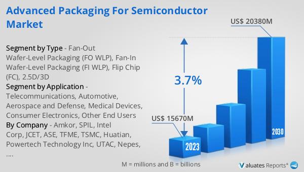
The worldwide market for Advanced Packaging for Semiconductor was valued at approximately $16.9 billion in 2024 and is anticipated to expand to a revised size of around $21.78 billion by 2031, reflecting a compound annual growth rate (CAGR) of 3.7% over the forecast period. In parallel, the global semiconductor market was estimated at about $579 billion in 2022 and is projected to reach approximately $790 billion by 2029, growing at a CAGR of 6% during the same period. This growth is indicative of the increasing demand for advanced semiconductor solutions driven by the rapid technological advancements and the need for more efficient, high-performance electronic devices. As industries such as telecommunications, automotive, aerospace, defense, medical devices, and consumer electronics continue to evolve, the demand for advanced packaging solutions is expected to rise. These solutions are crucial for enhancing the performance, efficiency, and functionality of semiconductor devices, enabling the development of smaller, faster, and more efficient products. The continuous innovation in advanced packaging technologies is expected to drive growth in the global semiconductor market, meeting the evolving needs of various industries and contributing to the overall expansion of the market.
| Report Metric | Details |
| Report Name | Advanced Packaging for Semiconductor Market |
| Accounted market size in year | US$ 16900 million |
| Forecasted market size in 2031 | US$ 21780 million |
| CAGR | 3.7% |
| Base Year | year |
| Forecasted years | 2025 - 2031 |
| Segment by Type |
|
| Segment by Application |
|
| By Region |
|
| By Company | Amkor, SPIL, Intel Corp, JCET, ASE, TFME, TSMC, Huatian, Powertech Technology Inc, UTAC, Nepes, Walton Advanced Engineering, Kyocera, Chipbond, Chipmos |
| Forecast units | USD million in value |
| Report coverage | Revenue and volume forecast, company share, competitive landscape, growth factors and trends |


