What is Global Wafer Permanent Bonder Market?
The Global Wafer Permanent Bonder Market is a specialized segment within the semiconductor industry that focuses on the technology and equipment used to permanently bond wafers. Wafers are thin slices of semiconductor material, such as silicon, used in the fabrication of integrated circuits and other microdevices. The permanent bonding process is crucial as it ensures the structural integrity and functionality of these devices. This market encompasses various bonding techniques, including adhesive bonding, anodic bonding, and fusion bonding, each suited for different applications and materials. The demand for wafer permanent bonders is driven by the increasing complexity and miniaturization of electronic devices, which require more advanced and reliable bonding solutions. As technology evolves, the market is witnessing innovations aimed at improving bonding precision, speed, and efficiency. This market is integral to the production of a wide range of electronic components, from microelectromechanical systems (MEMS) to advanced packaging solutions, making it a vital part of the global electronics manufacturing ecosystem. The growth of this market is closely linked to the broader trends in the semiconductor industry, including the rise of the Internet of Things (IoT), artificial intelligence (AI), and the ongoing demand for smaller, faster, and more efficient electronic devices.
Fully Automatic, Semi Automatic in the Global Wafer Permanent Bonder Market:
In the Global Wafer Permanent Bonder Market, equipment is generally categorized into fully automatic and semi-automatic systems, each serving distinct needs based on the scale and precision required in semiconductor manufacturing. Fully automatic wafer bonders are designed for high-volume production environments where speed, precision, and minimal human intervention are critical. These systems are equipped with advanced robotics and software that allow for the seamless handling and alignment of wafers, ensuring consistent and high-quality bonds. The automation in these systems reduces the likelihood of human error, enhances throughput, and is ideal for large-scale manufacturing processes where uniformity and efficiency are paramount. Fully automatic systems are often integrated into larger production lines, contributing to streamlined operations and reduced labor costs. On the other hand, semi-automatic wafer bonders offer a balance between automation and manual control, making them suitable for smaller production runs or research and development settings. These systems provide operators with the flexibility to adjust parameters and intervene in the bonding process, which can be advantageous when dealing with complex or custom bonding requirements. Semi-automatic bonders are often used in applications where precision and customization are more critical than speed, such as in prototyping or specialized manufacturing processes. While they may not match the throughput of fully automatic systems, semi-automatic bonders offer greater adaptability and can be more cost-effective for certain applications. Both types of systems are essential to the wafer bonding market, catering to different segments of the semiconductor industry. The choice between fully automatic and semi-automatic systems often depends on factors such as production volume, budget, and the specific technical requirements of the bonding process. As the semiconductor industry continues to evolve, the demand for both types of systems is expected to grow, driven by the increasing complexity and diversity of electronic devices. Manufacturers are continually innovating to enhance the capabilities of both fully automatic and semi-automatic wafer bonders, focusing on improving precision, reducing cycle times, and expanding the range of materials and applications they can handle. This ongoing innovation is crucial to meeting the ever-changing demands of the semiconductor industry and ensuring the continued growth and competitiveness of the Global Wafer Permanent Bonder Market.
MEMS, Advanced Packaging, CIS, Others in the Global Wafer Permanent Bonder Market:
The Global Wafer Permanent Bonder Market plays a crucial role in several key areas of semiconductor manufacturing, including MEMS, advanced packaging, CIS, and other applications. In the realm of MEMS (Microelectromechanical Systems), wafer bonding is essential for creating devices that integrate mechanical and electrical components at a microscale. MEMS devices are used in a wide range of applications, from automotive sensors to medical devices, and require precise and reliable bonding techniques to ensure their functionality and durability. The permanent bonding process in MEMS manufacturing often involves techniques such as anodic bonding or fusion bonding, which provide the necessary strength and stability for these intricate devices. In advanced packaging, wafer bonding is used to create multi-layered structures that enhance the performance and functionality of semiconductor devices. This includes techniques like wafer-level packaging and 3D integration, which allow for the stacking of multiple chips to increase processing power and reduce the overall size of electronic devices. The demand for advanced packaging solutions is driven by the need for smaller, faster, and more energy-efficient devices, making wafer bonding a critical component of this market. In the area of CIS (CMOS Image Sensors), wafer bonding is used to improve the performance and sensitivity of image sensors, which are widely used in cameras, smartphones, and other imaging applications. The bonding process helps to enhance the light sensitivity and resolution of these sensors, enabling better image quality and performance. Beyond these specific applications, wafer bonding is also used in a variety of other areas, including power electronics, RF devices, and optoelectronics. Each of these applications requires specialized bonding techniques and equipment to meet the unique demands of the market. As technology continues to advance, the Global Wafer Permanent Bonder Market is expected to grow, driven by the increasing complexity and diversity of electronic devices and the ongoing demand for more advanced and reliable bonding solutions.
Global Wafer Permanent Bonder Market Outlook:
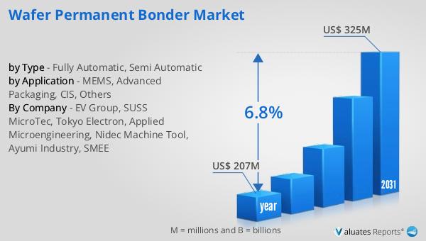
The outlook for the Global Wafer Permanent Bonder Market indicates a promising growth trajectory over the coming years. In 2024, the market was valued at approximately US$ 207 million, reflecting its significance in the semiconductor industry. Looking ahead to 2031, the market is projected to expand to a revised size of US$ 325 million. This growth is expected to occur at a compound annual growth rate (CAGR) of 6.8% during the forecast period. This upward trend underscores the increasing demand for advanced wafer bonding solutions, driven by the rapid evolution of electronic devices and the semiconductor industry as a whole. The market's expansion is likely fueled by the continuous advancements in technology, which necessitate more sophisticated and reliable bonding techniques. As electronic devices become more complex and miniaturized, the need for precise and efficient wafer bonding solutions becomes even more critical. This growth trajectory highlights the importance of the Global Wafer Permanent Bonder Market in supporting the development and production of cutting-edge semiconductor devices. The market's robust growth prospects reflect its vital role in enabling the next generation of electronic innovations, ensuring that manufacturers can meet the ever-increasing demands for smaller, faster, and more efficient devices.
| Report Metric | Details |
| Report Name | Wafer Permanent Bonder Market |
| Accounted market size in year | US$ 207 million |
| Forecasted market size in 2031 | US$ 325 million |
| CAGR | 6.8% |
| Base Year | year |
| Forecasted years | 2025 - 2031 |
| by Type |
|
| by Application |
|
| Production by Region |
|
| Consumption by Region |
|
| By Company | EV Group, SUSS MicroTec, Tokyo Electron, Applied Microengineering, Nidec Machine Tool, Ayumi Industry, SMEE |
| Forecast units | USD million in value |
| Report coverage | Revenue and volume forecast, company share, competitive landscape, growth factors and trends |