What is Atomic Force Microscopy (AFM)- Global Market?
Atomic Force Microscopy (AFM) is a sophisticated technique used to analyze surfaces at the nanoscale level, providing detailed topographical data. This technology is pivotal in various scientific and industrial fields due to its ability to deliver high-resolution images and measurements of surface characteristics. The global market for AFM is expanding as industries increasingly recognize its potential for innovation and quality control. AFM operates by scanning a sharp probe over a surface to measure forces between the probe and the sample, which are then used to construct a detailed image. This method is non-destructive, allowing for the examination of delicate samples without causing damage. The versatility of AFM makes it applicable in numerous sectors, including materials science, biology, and electronics, where understanding surface properties is crucial. As technology advances, the demand for more precise and reliable surface analysis tools like AFM continues to grow, driving market expansion. The global market for AFM is projected to see significant growth, reflecting its importance in research and development across various industries. This growth is supported by ongoing advancements in AFM technology, which enhance its capabilities and applications.
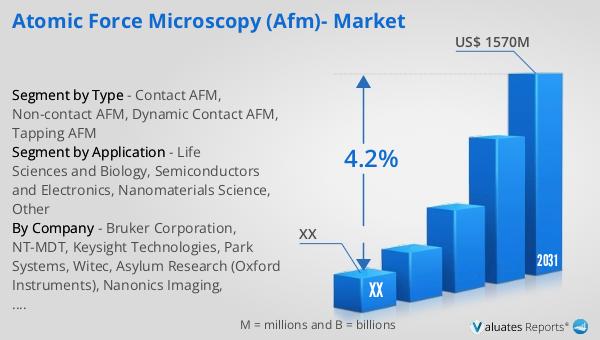
Contact AFM, Non-contact AFM, Dynamic Contact AFM, Tapping AFM in the Atomic Force Microscopy (AFM)- Global Market:
Atomic Force Microscopy (AFM) encompasses several modes of operation, each tailored to specific applications and sample types. Contact AFM is the most straightforward mode, where the probe maintains constant contact with the sample surface. This method is ideal for measuring surface roughness and mechanical properties but can sometimes damage soft samples due to the continuous contact. Non-contact AFM, on the other hand, operates by keeping the probe slightly above the surface, detecting forces without direct contact. This mode is less likely to damage delicate samples and is suitable for imaging soft materials or biological specimens. Dynamic Contact AFM, also known as intermittent contact or tapping mode, involves the probe oscillating near the surface, making intermittent contact. This approach reduces lateral forces, minimizing damage while providing high-resolution images. Tapping AFM is particularly useful for samples that are easily deformed or damaged, such as polymers and biological samples. Each of these modes offers unique advantages and is selected based on the specific requirements of the sample and the information needed. The global market for AFM is driven by the diverse applications of these modes, as they provide critical insights into material properties at the nanoscale. As industries continue to innovate and develop new materials, the demand for precise surface characterization tools like AFM is expected to rise. The versatility of AFM modes allows researchers and engineers to tailor their approach to the specific needs of their projects, enhancing the value of AFM in various fields. The ability to choose the appropriate mode for a given application ensures that AFM remains a vital tool in scientific research and industrial applications. As the global market for AFM grows, the development of new modes and enhancements to existing ones will likely continue, further expanding the capabilities and applications of this powerful technology.
Life Sciences and Biology, Semiconductors and Electronics, Nanomaterials Science, Other in the Atomic Force Microscopy (AFM)- Global Market:
Atomic Force Microscopy (AFM) is widely used across several key areas, each benefiting from its ability to provide detailed surface analysis at the nanoscale. In life sciences and biology, AFM is instrumental in studying the structure and properties of biological molecules, cells, and tissues. It allows researchers to visualize the surface of biological samples in their natural state, providing insights into cellular processes and molecular interactions. This capability is crucial for advancing our understanding of diseases and developing new medical treatments. In the semiconductor and electronics industries, AFM is used to analyze the surface properties of materials used in electronic devices. It helps in quality control and the development of new materials with improved performance characteristics. AFM's ability to measure surface roughness and detect defects at the nanoscale is essential for ensuring the reliability and efficiency of electronic components. In nanomaterials science, AFM is used to characterize the properties of nanomaterials, such as nanoparticles and nanotubes. It provides valuable information on the size, shape, and surface properties of these materials, which is critical for their development and application in various fields. Other areas where AFM is used include materials science, where it helps in the study of polymers, metals, and ceramics, and environmental science, where it is used to analyze soil and water samples. The global market for AFM is driven by its wide range of applications and the growing demand for precise surface analysis tools in these fields. As industries continue to innovate and develop new materials and technologies, the need for advanced characterization techniques like AFM is expected to increase. The versatility and precision of AFM make it an indispensable tool in scientific research and industrial applications, driving its growth in the global market.
Atomic Force Microscopy (AFM)- Global Market Outlook:
The global market for Atomic Force Microscopy (AFM) was valued at approximately $1,182 million in 2024. It is anticipated to grow to a revised size of around $1,570 million by 2031, reflecting a compound annual growth rate (CAGR) of 4.2% during the forecast period from 2025 to 2031. This growth is indicative of the increasing recognition of AFM's capabilities and its expanding applications across various industries. The steady rise in market value underscores the importance of AFM in providing high-resolution surface analysis, which is crucial for innovation and quality control in numerous fields. As industries continue to evolve and demand more precise and reliable analytical tools, the role of AFM is expected to become even more significant. The projected growth in the AFM market is supported by ongoing advancements in technology, which enhance its capabilities and broaden its applications. This trend highlights the growing importance of AFM in research and development, as well as its potential to drive innovation in various sectors. The increasing demand for AFM is a testament to its value as a versatile and powerful tool for surface characterization, making it an essential component of modern scientific and industrial practices.
| Report Metric | Details |
| Report Name | Atomic Force Microscopy (AFM)- Market |
| Forecasted market size in 2031 | US$ 1570 million |
| CAGR | 4.2% |
| Forecasted years | 2025 - 2031 |
| Segment by Type |
|
| Segment by Application |
|
| By Region |
|
| By Company | Bruker Corporation, NT-MDT, Keysight Technologies, Park Systems, Witec, Asylum Research (Oxford Instruments), Nanonics Imaging, Nanosurf, Hitachi High-Technologies, Anasys Instruments, RHK Technology, A.P.E. Research |
| Forecast units | USD million in value |
| Report coverage | Revenue and volume forecast, company share, competitive landscape, growth factors and trends |


