What is Global Semiconductor Wafer Microscope Market?
The Global Semiconductor Wafer Microscope Market is a specialized segment within the broader semiconductor industry, focusing on the tools and technologies used to inspect and analyze semiconductor wafers. These microscopes are essential for ensuring the quality and precision of semiconductor wafers, which are the foundational components of electronic devices. As the demand for smaller, more powerful, and energy-efficient electronic devices grows, so does the need for advanced inspection tools like semiconductor wafer microscopes. These microscopes help in identifying defects, ensuring uniformity, and maintaining the high standards required in semiconductor manufacturing. The market encompasses various types of microscopes, each designed to meet specific inspection needs, from surface inspection to more complex analyses. The growth of this market is driven by technological advancements, increasing demand for consumer electronics, and the continuous evolution of semiconductor technology. As industries such as automotive, telecommunications, and consumer electronics expand, the need for high-quality semiconductor wafers and, consequently, the microscopes that inspect them, becomes increasingly critical. This market is characterized by innovation, with companies investing heavily in research and development to produce more efficient and accurate inspection tools.
Boom Stand Microscope, Large Stand Microscope, Others in the Global Semiconductor Wafer Microscope Market:
The Global Semiconductor Wafer Microscope Market includes various types of microscopes, each serving distinct purposes in the inspection and analysis of semiconductor wafers. Among these, the Boom Stand Microscope is a versatile tool known for its flexibility and ease of use. It is designed with an adjustable arm that allows users to position the microscope over large areas, making it ideal for inspecting larger wafers or multiple wafers simultaneously. This type of microscope is particularly useful in environments where space is limited or where the inspection needs to be conducted over a wide area. Its adaptability makes it a popular choice in many semiconductor manufacturing facilities. On the other hand, the Large Stand Microscope is built for stability and precision. It is typically used in applications where high magnification and detailed analysis are required. This microscope is mounted on a sturdy stand, providing a stable platform for examining wafers at high resolutions. It is often used in research and development settings, where detailed inspection and analysis are crucial. The Large Stand Microscope is favored for its ability to provide clear and detailed images, which are essential for identifying minute defects or irregularities in semiconductor wafers. In addition to these, there are other types of microscopes used in the semiconductor wafer inspection market. These include digital microscopes, which offer the advantage of capturing and storing images for further analysis. Digital microscopes are increasingly popular due to their ability to integrate with computer systems, allowing for enhanced image processing and analysis. They are particularly useful in automated inspection systems, where speed and accuracy are paramount. Another category is the stereo microscope, which provides a three-dimensional view of the wafer surface. This type of microscope is beneficial for inspecting the topography of the wafer, allowing for a more comprehensive analysis of its surface features. Stereo microscopes are often used in conjunction with other types of microscopes to provide a more complete picture of the wafer's condition. Each type of microscope in the Global Semiconductor Wafer Microscope Market plays a crucial role in ensuring the quality and reliability of semiconductor wafers. As the demand for more advanced and efficient electronic devices continues to grow, the need for precise and reliable inspection tools becomes increasingly important. Manufacturers in this market are continually innovating, developing new technologies and features to meet the evolving needs of the semiconductor industry. This ongoing innovation is essential for maintaining the high standards required in semiconductor manufacturing and for supporting the continued growth of the electronics industry.
Surface Inspection, Optical, Automated, Scanning Acoustic, Others in the Global Semiconductor Wafer Microscope Market:
The Global Semiconductor Wafer Microscope Market plays a vital role in various inspection areas, each with its unique applications and benefits. Surface inspection is one of the primary uses of these microscopes, focusing on identifying defects and irregularities on the wafer's surface. This process is crucial for ensuring the quality and reliability of semiconductor wafers, as surface defects can significantly impact the performance of electronic devices. Surface inspection microscopes are designed to provide high-resolution images, allowing for detailed analysis of the wafer's surface features. These microscopes are essential for detecting even the smallest defects, ensuring that only wafers meeting the highest quality standards proceed to the next stages of production. Optical inspection is another critical area where semiconductor wafer microscopes are used. This process involves using light to examine the wafer's surface and internal structures. Optical microscopes are equipped with advanced lenses and lighting systems, enabling them to capture detailed images of the wafer. This type of inspection is particularly useful for identifying defects that may not be visible to the naked eye, such as micro-cracks or contamination. Optical inspection is a non-destructive method, making it ideal for use in quality control processes where preserving the integrity of the wafer is essential. Automated inspection systems are becoming increasingly prevalent in the semiconductor industry, driven by the need for faster and more efficient inspection processes. These systems integrate advanced microscopes with computer software, allowing for real-time analysis and defect detection. Automated inspection systems are capable of processing large volumes of wafers quickly, making them ideal for high-volume manufacturing environments. They offer the advantage of consistency and accuracy, reducing the likelihood of human error and ensuring that all wafers meet the required quality standards. Scanning Acoustic Microscopy (SAM) is another technique used in the inspection of semiconductor wafers. This method uses high-frequency sound waves to examine the internal structures of the wafer, providing valuable information about its composition and integrity. SAM is particularly useful for detecting internal defects, such as voids or delaminations, that may not be visible through optical inspection. This technique is non-destructive and provides a comprehensive analysis of the wafer's internal features, making it an essential tool in quality control processes. In addition to these specific inspection areas, semiconductor wafer microscopes are used in various other applications, each contributing to the overall quality and reliability of semiconductor wafers. These microscopes are essential tools in the semiconductor industry, providing the precision and accuracy needed to ensure that wafers meet the highest quality standards. As the demand for more advanced and efficient electronic devices continues to grow, the importance of reliable and accurate inspection tools becomes increasingly critical. The Global Semiconductor Wafer Microscope Market is characterized by continuous innovation, with manufacturers developing new technologies and features to meet the evolving needs of the industry. This ongoing innovation is essential for supporting the continued growth of the semiconductor industry and for ensuring the quality and reliability of the electronic devices that rely on these critical components.
Global Semiconductor Wafer Microscope Market Outlook:
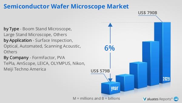
In 2022, the global semiconductor market was valued at approximately $579 billion, and it is anticipated to reach around $790 billion by 2029. This growth represents a compound annual growth rate (CAGR) of 6% over the forecast period. The expansion of this market is driven by several factors, including the increasing demand for consumer electronics, advancements in technology, and the growing need for more efficient and powerful electronic devices. As industries such as automotive, telecommunications, and consumer electronics continue to expand, the demand for high-quality semiconductor components is expected to rise. This growth is also supported by the continuous innovation and development within the semiconductor industry, as manufacturers strive to produce more advanced and efficient products. The increasing adoption of technologies such as artificial intelligence, the Internet of Things (IoT), and 5G is also contributing to the growth of the semiconductor market, as these technologies require advanced semiconductor components to function effectively. As the market continues to grow, the importance of reliable and accurate inspection tools, such as semiconductor wafer microscopes, becomes increasingly critical. These tools play a vital role in ensuring the quality and reliability of semiconductor wafers, which are essential for the production of high-quality electronic devices. The Global Semiconductor Wafer Microscope Market is expected to continue its growth trajectory, driven by the increasing demand for advanced inspection tools and the continuous innovation within the semiconductor industry.
| Report Metric | Details |
| Report Name | Semiconductor Wafer Microscope Market |
| Accounted market size in year | US$ 579 billion |
| Forecasted market size in 2029 | US$ 790 billion |
| CAGR | 6% |
| Base Year | year |
| Forecasted years | 2025 - 2029 |
| by Type |
|
| by Application |
|
| Production by Region |
|
| Consumption by Region |
|
| By Company | FormFactor, PVA TePla, AmScope, LEICA, OLYMPUS, Nikon, Meiji Techno America |
| Forecast units | USD million in value |
| Report coverage | Revenue and volume forecast, company share, competitive landscape, growth factors and trends |


