What is Global EUV Lithography Pellicle Market?
The Global EUV Lithography Pellicle Market is a specialized segment within the semiconductor industry, focusing on the production and utilization of pellicles for extreme ultraviolet (EUV) lithography. EUV lithography is a cutting-edge technology used in the manufacturing of semiconductors, allowing for the creation of smaller and more efficient microchips. Pellicles are thin, transparent membranes that protect photomasks during the lithography process, preventing defects caused by particles. The demand for EUV lithography pellicles is driven by the increasing need for advanced semiconductor devices in various applications, including consumer electronics, automotive, and telecommunications. As the semiconductor industry continues to push the boundaries of miniaturization and performance, the role of EUV lithography pellicles becomes increasingly critical. These pellicles must meet stringent requirements for durability, transparency, and compatibility with EUV wavelengths to ensure the production of high-quality microchips. The market is characterized by ongoing research and development efforts to enhance pellicle performance and reduce costs, as well as collaborations between semiconductor manufacturers and pellicle suppliers to address the challenges of EUV lithography.
Transmittance: >90%, Transmittance: ≤ 90% in the Global EUV Lithography Pellicle Market:
In the Global EUV Lithography Pellicle Market, transmittance is a crucial factor that determines the efficiency and effectiveness of pellicles used in the lithography process. Transmittance refers to the percentage of EUV light that passes through the pellicle without being absorbed or reflected. Pellicles with a transmittance of greater than 90% are highly sought after because they allow more EUV light to reach the photomask, which is essential for precise and accurate patterning of semiconductor wafers. High transmittance pellicles contribute to improved lithography performance, enabling the production of smaller and more complex semiconductor devices. On the other hand, pellicles with a transmittance of 90% or less may result in reduced lithography efficiency, as less EUV light reaches the photomask, potentially leading to defects or inaccuracies in the final semiconductor product. The development of pellicles with high transmittance is a significant focus for manufacturers, as it directly impacts the quality and yield of semiconductor production. Achieving high transmittance requires advanced materials and manufacturing techniques to ensure that the pellicle is both transparent and durable enough to withstand the harsh conditions of the EUV lithography process. The ongoing research and development efforts in this area aim to optimize the balance between transmittance, durability, and cost, making high-performance pellicles more accessible to semiconductor manufacturers. As the demand for advanced semiconductor devices continues to grow, the importance of high transmittance pellicles in the EUV lithography process cannot be overstated. Manufacturers are investing in innovative solutions to enhance pellicle performance, including the use of novel materials and coatings that improve transmittance while maintaining structural integrity. These advancements are critical for meeting the evolving needs of the semiconductor industry and ensuring the continued progress of EUV lithography technology. The competition among pellicle manufacturers is intense, with companies striving to develop products that offer superior transmittance and reliability. Collaborations between semiconductor manufacturers and pellicle suppliers are also common, as they work together to address the challenges of EUV lithography and develop solutions that meet the specific requirements of different applications. The success of these efforts will play a pivotal role in shaping the future of the Global EUV Lithography Pellicle Market and the broader semiconductor industry.
Integrated Device Manufacturer (IDM), Foundry in the Global EUV Lithography Pellicle Market:
The Global EUV Lithography Pellicle Market plays a vital role in the operations of Integrated Device Manufacturers (IDMs) and foundries, which are key players in the semiconductor industry. IDMs are companies that design, manufacture, and sell their own semiconductor products, while foundries specialize in manufacturing semiconductors for other companies. Both types of organizations rely on EUV lithography pellicles to ensure the quality and efficiency of their semiconductor production processes. For IDMs, the use of high-quality EUV lithography pellicles is essential for maintaining competitive advantage and meeting the demands of their customers. These companies often produce a wide range of semiconductor products, from microprocessors to memory chips, and require pellicles that can support the production of diverse and complex designs. High transmittance pellicles are particularly important for IDMs, as they enable the precise patterning of semiconductor wafers, resulting in higher performance and reliability of the final products. By investing in advanced pellicle technologies, IDMs can enhance their production capabilities and deliver cutting-edge semiconductor solutions to the market. Foundries, on the other hand, focus on providing manufacturing services to other companies, including fabless semiconductor firms that design chips but do not have their own manufacturing facilities. For foundries, the ability to offer high-quality and efficient semiconductor production is crucial for attracting and retaining clients. EUV lithography pellicles with high transmittance are a key component of this capability, as they ensure the accuracy and consistency of the lithography process. Foundries must continuously invest in the latest pellicle technologies to meet the evolving needs of their clients and maintain their position in the competitive semiconductor manufacturing landscape. The collaboration between pellicle manufacturers and foundries is essential for developing solutions that address the specific challenges of EUV lithography and support the production of advanced semiconductor devices. Both IDMs and foundries face the challenge of balancing cost and performance when selecting EUV lithography pellicles. While high transmittance pellicles offer significant advantages in terms of lithography efficiency and product quality, they can also be more expensive to produce. As a result, companies must carefully evaluate their options and consider factors such as production volume, product complexity, and customer requirements when making purchasing decisions. The ongoing advancements in pellicle technology, including the development of cost-effective materials and manufacturing processes, are helping to address these challenges and make high-performance pellicles more accessible to a wider range of semiconductor manufacturers. The Global EUV Lithography Pellicle Market is poised to play an increasingly important role in the semiconductor industry as IDMs and foundries continue to push the boundaries of technology and innovation. By leveraging the latest pellicle technologies, these companies can enhance their production capabilities, improve product quality, and meet the growing demand for advanced semiconductor devices. The collaboration between pellicle manufacturers, IDMs, and foundries will be critical for driving the future growth and success of the market, as they work together to overcome the challenges of EUV lithography and deliver cutting-edge solutions to the industry.
Global EUV Lithography Pellicle Market Outlook:
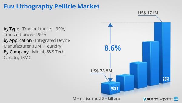
In 2024, the global market for EUV Lithography Pellicles was valued at approximately $78.8 million. This market is anticipated to expand significantly, reaching an estimated size of $171 million by 2031, with a compound annual growth rate (CAGR) of 8.6% throughout the forecast period. This growth trajectory underscores the increasing importance and demand for EUV lithography pellicles in the semiconductor industry. A notable development in this market occurred in 2021 when a South Korean company, SS Tech, successfully developed a pellicle with a transmittance exceeding 90%. This advancement highlights the ongoing efforts within the industry to enhance pellicle performance and meet the stringent requirements of EUV lithography. The ability to achieve high transmittance is crucial for improving lithography efficiency and ensuring the production of high-quality semiconductor devices. As the market continues to evolve, innovations like those from SS Tech are expected to play a pivotal role in shaping the future of EUV lithography pellicles and their applications in the semiconductor industry. The focus on improving transmittance, durability, and cost-effectiveness will drive further advancements and contribute to the overall growth and success of the Global EUV Lithography Pellicle Market.
| Report Metric | Details |
| Report Name | EUV Lithography Pellicle Market |
| Accounted market size in year | US$ 78.8 million |
| Forecasted market size in 2031 | US$ 171 million |
| CAGR | 8.6% |
| Base Year | year |
| Forecasted years | 2025 - 2031 |
| by Type |
|
| by Application |
|
| Production by Region |
|
| Consumption by Region |
|
| By Company | Mitsui, S&S Tech, Canatu, TSMC |
| Forecast units | USD million in value |
| Report coverage | Revenue and volume forecast, company share, competitive landscape, growth factors and trends |


