What is Global Cleaning Equipment for Single Wafer Market?
The Global Cleaning Equipment for Single Wafer Market refers to the specialized machinery and tools used in the semiconductor industry to clean individual wafers. These wafers are thin slices of semiconductor material, such as silicon, used in the fabrication of integrated circuits and other microdevices. The cleaning process is crucial because even the smallest particles or contaminants can affect the performance and yield of semiconductor devices. The equipment used for cleaning single wafers is designed to remove these impurities without damaging the delicate wafer surfaces. This market is driven by the increasing demand for semiconductors in various applications, including consumer electronics, automotive, and telecommunications. As technology advances, the need for more precise and efficient cleaning solutions grows, making this market an essential component of the semiconductor manufacturing process. The equipment typically involves processes such as chemical cleaning, physical scrubbing, and drying, all tailored to ensure the highest level of cleanliness and performance. The market is characterized by continuous innovation, with manufacturers striving to develop more effective and environmentally friendly cleaning solutions to meet the evolving needs of the semiconductor industry.
Wafer Size 50mm-200mm, Wafer Size 300mm, Others in the Global Cleaning Equipment for Single Wafer Market:
In the Global Cleaning Equipment for Single Wafer Market, wafer sizes play a significant role in determining the type of equipment and processes used. Wafer sizes typically range from 50mm to 300mm, with each size presenting unique challenges and requirements. Wafers sized between 50mm and 200mm are often used in niche applications or older semiconductor manufacturing processes. These smaller wafers require specialized cleaning equipment that can handle their delicate nature while ensuring thorough removal of contaminants. The cleaning process for these wafers often involves a combination of chemical and mechanical methods to achieve the desired level of cleanliness without causing damage. On the other hand, 300mm wafers are the standard in modern semiconductor manufacturing, particularly for high-volume production. The larger surface area of these wafers necessitates advanced cleaning technologies that can efficiently and effectively remove particles and residues. Equipment designed for 300mm wafers often incorporates sophisticated automation and control systems to ensure consistent results across large batches. Additionally, the cleaning process for these wafers may involve multiple stages, including pre-cleaning, main cleaning, and post-cleaning, each tailored to address specific types of contaminants. Beyond the standard wafer sizes, there are also other sizes used in specialized applications, such as research and development or custom semiconductor devices. These wafers may require bespoke cleaning solutions that can accommodate their unique dimensions and material properties. The cleaning equipment for these wafers must be highly adaptable and capable of handling a wide range of cleaning challenges. Overall, the Global Cleaning Equipment for Single Wafer Market is characterized by a diverse array of equipment and technologies, each designed to meet the specific needs of different wafer sizes and applications. As the semiconductor industry continues to evolve, the demand for more efficient and effective cleaning solutions will drive further innovation in this market.
MEMS, CIS, Memory, RF devices, LED, Logic, Others in the Global Cleaning Equipment for Single Wafer Market:
The Global Cleaning Equipment for Single Wafer Market finds its usage across various applications, including MEMS, CIS, Memory, RF devices, LED, Logic, and others. In the realm of Micro-Electro-Mechanical Systems (MEMS), cleaning equipment is crucial for ensuring the precision and reliability of these tiny devices. MEMS are used in a wide range of applications, from automotive sensors to medical devices, and any contamination can lead to significant performance issues. The cleaning process for MEMS often involves delicate handling and precise control to avoid damaging the intricate structures. In the case of CMOS Image Sensors (CIS), which are widely used in cameras and imaging devices, cleaning equipment plays a vital role in maintaining image quality. Any particles or residues on the wafer surface can lead to defects in the final product, affecting the sensor's performance. The cleaning process for CIS wafers typically involves multiple stages to ensure the highest level of cleanliness. For memory devices, such as DRAM and NAND flash, cleaning equipment is essential for achieving high yields and reliability. These devices require extremely clean surfaces to function correctly, and any contamination can lead to data errors or device failure. The cleaning process for memory wafers often involves advanced chemical and physical methods to remove even the smallest particles. RF devices, used in wireless communication systems, also rely on clean wafer surfaces to ensure optimal performance. The cleaning equipment for these devices must be capable of removing a wide range of contaminants, including organic residues and metallic particles. In the LED industry, cleaning equipment is used to ensure the efficiency and longevity of light-emitting diodes. Any contamination on the wafer surface can affect the LED's brightness and color consistency, making thorough cleaning essential. Finally, in the realm of logic devices, which form the backbone of modern computing, cleaning equipment is critical for achieving high performance and reliability. The cleaning process for logic wafers often involves a combination of chemical and mechanical methods to ensure the removal of all contaminants. Overall, the Global Cleaning Equipment for Single Wafer Market plays a vital role in ensuring the quality and performance of a wide range of semiconductor devices, each with its unique cleaning requirements.
Global Cleaning Equipment for Single Wafer Market Outlook:
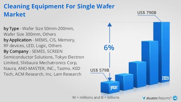
The global semiconductor market was valued at approximately $579 billion in 2022, and it is anticipated to reach around $790 billion by 2029, reflecting a compound annual growth rate (CAGR) of 6% over the forecast period. This growth is driven by the increasing demand for semiconductors across various industries, including consumer electronics, automotive, telecommunications, and industrial applications. As technology continues to advance, the need for more powerful and efficient semiconductor devices is growing, leading to increased investments in research and development. The expansion of the Internet of Things (IoT), artificial intelligence, and 5G technology are also contributing to the rising demand for semiconductors. Additionally, the shift towards electric vehicles and renewable energy solutions is further fueling the growth of the semiconductor market. As a result, the demand for advanced semiconductor manufacturing equipment, including cleaning equipment for single wafers, is expected to increase. This growth presents significant opportunities for companies operating in the semiconductor industry, as they strive to develop innovative solutions to meet the evolving needs of their customers. Overall, the global semiconductor market is poised for substantial growth in the coming years, driven by technological advancements and increasing demand across various sectors.
| Report Metric | Details |
| Report Name | Cleaning Equipment for Single Wafer Market |
| Accounted market size in year | US$ 579 billion |
| Forecasted market size in 2029 | US$ 790 billion |
| CAGR | 6% |
| Base Year | year |
| Forecasted years | 2025 - 2029 |
| by Type |
|
| by Application |
|
| Production by Region |
|
| Consumption by Region |
|
| By Company | SEMES, SCREEN Semiconductor Solutions, Tokyo Electron Limited, Shibaura Mechatronics Corp, Naura, ANO-MASTER, INC., Tazmo, KED Tech, ACM Research, Inc, Lam Research |
| Forecast units | USD million in value |
| Report coverage | Revenue and volume forecast, company share, competitive landscape, growth factors and trends |


