What is Global Automatic Wafer Handling System Market?
The Global Automatic Wafer Handling System Market is a specialized segment within the semiconductor industry that focuses on the automation of wafer handling processes. Wafers, which are thin slices of semiconductor material, are essential components in the manufacturing of electronic devices. The automatic wafer handling systems are designed to transport, align, and process these wafers with high precision and efficiency, minimizing human intervention and reducing the risk of contamination. These systems are crucial in semiconductor fabrication plants, where they help streamline operations, improve yield, and enhance overall productivity. The market for these systems is driven by the increasing demand for semiconductors in various applications, such as consumer electronics, automotive, and telecommunications. As technology advances, the need for more sophisticated and efficient wafer handling solutions continues to grow, making this market an integral part of the semiconductor manufacturing ecosystem. The market is characterized by rapid technological advancements and a high level of competition among key players striving to offer innovative solutions that meet the evolving needs of the semiconductor industry.
Atmospheric Transport Systems, Vacuum Transport Systems in the Global Automatic Wafer Handling System Market:
Atmospheric Transport Systems and Vacuum Transport Systems are two critical components of the Global Automatic Wafer Handling System Market, each serving distinct functions in the semiconductor manufacturing process. Atmospheric Transport Systems operate in environments where wafers are exposed to ambient air. These systems are typically used in processes that do not require a vacuum, such as wafer loading and unloading, inspection, and certain types of cleaning. They are designed to handle wafers delicately to prevent damage and contamination, ensuring that the wafers remain in pristine condition throughout the handling process. The systems often incorporate advanced robotics and sensors to achieve precise movement and alignment of wafers, which is crucial for maintaining the integrity of the semiconductor manufacturing process. On the other hand, Vacuum Transport Systems are used in processes that require a controlled environment, free from air and other contaminants. These systems are essential for processes such as etching, deposition, and lithography, where even the slightest contamination can lead to defects in the semiconductor devices. Vacuum Transport Systems create a vacuum environment around the wafers, preventing exposure to air and other potential contaminants. They are equipped with sophisticated vacuum pumps and sealing mechanisms to maintain the vacuum conditions necessary for these sensitive processes. Both Atmospheric and Vacuum Transport Systems are integral to the efficiency and effectiveness of semiconductor manufacturing. They are designed to work seamlessly with other equipment in the fabrication plant, ensuring smooth and uninterrupted production. The choice between atmospheric and vacuum systems depends on the specific requirements of the manufacturing process, with some facilities utilizing a combination of both to optimize their operations. As the demand for semiconductors continues to rise, driven by advancements in technology and the proliferation of electronic devices, the need for efficient and reliable wafer handling systems becomes increasingly important. Manufacturers are continually innovating to develop systems that offer greater precision, speed, and flexibility, enabling semiconductor companies to meet the growing demands of the market. The competition in the Global Automatic Wafer Handling System Market is intense, with companies investing heavily in research and development to create cutting-edge solutions that cater to the diverse needs of the semiconductor industry. As a result, the market is characterized by rapid technological advancements and a constant push towards automation and efficiency.
300mm Wafer Size, 200mm Wafer Size, Others in the Global Automatic Wafer Handling System Market:
The Global Automatic Wafer Handling System Market plays a crucial role in the semiconductor industry, particularly in the handling of wafers of various sizes, including 300mm, 200mm, and others. The 300mm wafer size is the most common in modern semiconductor manufacturing, as it allows for more chips to be produced from a single wafer, thereby increasing efficiency and reducing costs. Automatic wafer handling systems for 300mm wafers are designed to manage the larger size and weight of these wafers, ensuring precise alignment and movement throughout the manufacturing process. These systems are equipped with advanced robotics and sensors to handle the wafers delicately, minimizing the risk of damage and contamination. The 200mm wafer size, while less common than the 300mm, is still widely used in certain applications, particularly in the production of analog and power devices. Automatic wafer handling systems for 200mm wafers are designed to accommodate the smaller size and different handling requirements of these wafers. They offer similar features to the 300mm systems, such as precision alignment and contamination control, but are optimized for the specific needs of 200mm wafer processing. In addition to 300mm and 200mm wafers, the Global Automatic Wafer Handling System Market also caters to other wafer sizes, which are used in niche applications or in older manufacturing facilities. These systems are designed to be versatile and adaptable, capable of handling a range of wafer sizes and types. This flexibility is essential for semiconductor manufacturers who need to produce a variety of products to meet the diverse demands of the market. The ability to efficiently handle different wafer sizes is a key factor in the competitiveness of semiconductor companies, as it allows them to optimize their production processes and reduce costs. As the semiconductor industry continues to evolve, driven by advancements in technology and the increasing demand for electronic devices, the need for efficient and reliable wafer handling systems becomes even more critical. Manufacturers are continually innovating to develop systems that offer greater precision, speed, and flexibility, enabling semiconductor companies to meet the growing demands of the market. The competition in the Global Automatic Wafer Handling System Market is intense, with companies investing heavily in research and development to create cutting-edge solutions that cater to the diverse needs of the semiconductor industry. As a result, the market is characterized by rapid technological advancements and a constant push towards automation and efficiency.
Global Automatic Wafer Handling System Market Outlook:
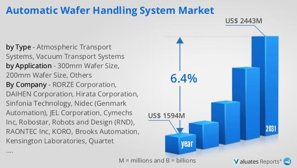
In 2024, the global market for Automatic Wafer Handling Systems was valued at approximately $1,594 million, with projections indicating it will expand to around $2,443 million by 2031, reflecting a compound annual growth rate (CAGR) of 6.4% over the forecast period. Notably, the top ten companies in this sector dominate with over 80% market share. In parallel, the semiconductor market was valued at $526.8 billion in 2023 and is anticipated to grow to $780.7 billion by 2030. Our research suggests that the global semiconductor manufacturing wafer fabrication market is expected to increase from $251.7 billion in 2023 to $506.5 billion by 2030, achieving a CAGR of 40.49% during this period. This growth underscores the critical role of Automatic Wafer Handling Systems in supporting the expanding semiconductor industry. As demand for semiconductors continues to rise, driven by technological advancements and the proliferation of electronic devices, the need for efficient and reliable wafer handling systems becomes increasingly important. Manufacturers are continually innovating to develop systems that offer greater precision, speed, and flexibility, enabling semiconductor companies to meet the growing demands of the market. The competition in the Global Automatic Wafer Handling System Market is intense, with companies investing heavily in research and development to create cutting-edge solutions that cater to the diverse needs of the semiconductor industry. As a result, the market is characterized by rapid technological advancements and a constant push towards automation and efficiency.
| Report Metric | Details |
| Report Name | Automatic Wafer Handling System Market |
| Accounted market size in year | US$ 1594 million |
| Forecasted market size in 2031 | US$ 2443 million |
| CAGR | 6.4% |
| Base Year | year |
| Forecasted years | 2025 - 2031 |
| by Type |
|
| by Application |
|
| Production by Region |
|
| Consumption by Region |
|
| By Company | RORZE Corporation, DAIHEN Corporation, Hirata Corporation, Sinfonia Technology, Nidec (Genmark Automation), JEL Corporation, Cymechs Inc, Robostar, Robots and Design (RND), RAONTEC Inc, KORO, Brooks Automation, Kensington Laboratories, Quartet Mechanics, Milara Incorporated, Accuron Technologies (RECIF Technologies), Sanwa Engineering Corporation, HIWIN TECHNOLOGIES, Siasun Robot & Automation, Beijing Jingyi Automation Equipment Technology, Shanghai Guona Semiconductor, Shanghai Fortrend Technology, Shanghai MICSON Industrial Automation, Shanghai HIROKAWA, HongHu (Suzhou) Semiconductor Technology, Beijing Sineva Intelligent Machine, Wisdom Semiconductor Technology, Wuxi Xinghui Technology, Mindox Techno, PHT Inc., SK Enpulse, Huaxin (Jiaxing) Intelligent Manufacturing, Tazmo |
| Forecast units | USD million in value |
| Report coverage | Revenue and volume forecast, company share, competitive landscape, growth factors and trends |


