What is Global Semiconductor Wafer Inspection System Market?
The Global Semiconductor Wafer Inspection System Market is a crucial segment within the semiconductor industry, focusing on the inspection and quality assurance of semiconductor wafers. These wafers are thin slices of semiconductor material, such as silicon, used in the fabrication of integrated circuits and other microdevices. The inspection systems are designed to detect defects and irregularities on the wafer surface, ensuring that only high-quality wafers proceed to the next stages of production. This market is driven by the increasing demand for semiconductors in various applications, including consumer electronics, automotive, and telecommunications. As technology advances, the complexity of semiconductor devices increases, necessitating more sophisticated inspection systems. These systems employ various techniques, such as optical and electron beam inspection, to identify defects at microscopic levels. The market is characterized by continuous innovation, with companies investing in research and development to enhance the accuracy and efficiency of their inspection systems. The growth of the semiconductor industry, coupled with the need for high-quality wafers, is expected to drive the demand for wafer inspection systems in the coming years. This market plays a vital role in ensuring the reliability and performance of semiconductor devices.
EFEM Inspection System, AOI Inspection System in the Global Semiconductor Wafer Inspection System Market:
EFEM (Equipment Front End Module) Inspection Systems and AOI (Automated Optical Inspection) Systems are integral components of the Global Semiconductor Wafer Inspection System Market. EFEM Inspection Systems are designed to handle wafers in a clean and controlled environment, minimizing contamination and ensuring precise handling during the inspection process. These systems are equipped with advanced robotics and automation technologies, allowing for efficient and accurate wafer handling. EFEM systems are crucial in maintaining the integrity of the wafers, as even the slightest contamination can lead to defects in the final semiconductor product. The use of EFEM systems is particularly important in high-volume manufacturing environments, where speed and precision are critical. On the other hand, AOI Inspection Systems utilize optical technologies to inspect wafers for defects. These systems employ high-resolution cameras and sophisticated image processing algorithms to detect surface defects, such as scratches, particles, and pattern deviations. AOI systems are capable of inspecting wafers at various stages of the manufacturing process, from initial wafer production to final device assembly. The ability to identify defects early in the production process is crucial in reducing waste and improving yield. AOI systems are highly adaptable and can be customized to meet the specific needs of different semiconductor manufacturing processes. The integration of EFEM and AOI systems in the semiconductor wafer inspection process offers several advantages. Firstly, it enhances the overall efficiency of the inspection process by automating wafer handling and defect detection. This reduces the reliance on manual inspection, which can be time-consuming and prone to errors. Secondly, the use of advanced technologies in these systems ensures a high level of accuracy in defect detection, minimizing the risk of defective wafers reaching the market. This is particularly important in industries where the reliability of semiconductor devices is critical, such as automotive and aerospace. Moreover, the combination of EFEM and AOI systems allows for real-time monitoring and analysis of the inspection process. This enables manufacturers to quickly identify and address any issues that may arise, reducing downtime and improving overall productivity. The data collected by these systems can also be used to optimize the manufacturing process, leading to further improvements in yield and quality. In conclusion, EFEM and AOI Inspection Systems are essential components of the Global Semiconductor Wafer Inspection System Market. Their ability to automate and enhance the inspection process plays a crucial role in ensuring the quality and reliability of semiconductor devices. As the demand for semiconductors continues to grow, the importance of these systems in the manufacturing process is expected to increase. Manufacturers are likely to continue investing in advanced inspection technologies to meet the evolving needs of the semiconductor industry.
Foundries, Memory Manufacturers, Integrated Device Manufacturer(IDMs) in the Global Semiconductor Wafer Inspection System Market:
The Global Semiconductor Wafer Inspection System Market finds significant usage in various areas, including foundries, memory manufacturers, and Integrated Device Manufacturers (IDMs). Foundries are specialized semiconductor manufacturing plants that produce chips for other companies. These facilities rely heavily on wafer inspection systems to ensure the quality and reliability of the chips they produce. The inspection systems are used at various stages of the manufacturing process, from initial wafer production to final chip assembly. By identifying defects early in the process, foundries can reduce waste and improve yield, ultimately leading to cost savings and increased profitability. Memory manufacturers, on the other hand, focus on producing memory chips, such as DRAM and NAND flash. These chips are used in a wide range of applications, from smartphones to data centers. The quality and reliability of memory chips are critical, as even minor defects can lead to data loss or corruption. Wafer inspection systems play a crucial role in ensuring the quality of memory chips by detecting defects at the wafer level. This allows manufacturers to address any issues before the chips are assembled and shipped to customers. The use of advanced inspection technologies, such as AOI and EFEM systems, is particularly important in the production of high-density memory chips, where the margin for error is minimal. Integrated Device Manufacturers (IDMs) are companies that design, manufacture, and sell their own semiconductor products. These companies have a vested interest in ensuring the quality and reliability of their products, as any defects can have a significant impact on their reputation and bottom line. Wafer inspection systems are an essential tool for IDMs, allowing them to maintain high standards of quality throughout the manufacturing process. By identifying and addressing defects early, IDMs can reduce the risk of defective products reaching the market, ultimately protecting their brand and customer relationships. In addition to quality assurance, wafer inspection systems also play a role in process optimization for IDMs. The data collected by these systems can be used to identify trends and patterns in the manufacturing process, allowing IDMs to make informed decisions about process improvements. This can lead to increased efficiency, reduced costs, and improved product performance. As the semiconductor industry continues to evolve, the importance of wafer inspection systems in ensuring quality and optimizing processes is expected to grow. In summary, the Global Semiconductor Wafer Inspection System Market is a critical component of the semiconductor industry, with significant usage in foundries, memory manufacturers, and IDMs. These systems play a vital role in ensuring the quality and reliability of semiconductor products, while also providing valuable insights for process optimization. As the demand for semiconductors continues to rise, the importance of wafer inspection systems in the manufacturing process is expected to increase, driving further innovation and investment in this market.
Global Semiconductor Wafer Inspection System Market Outlook:
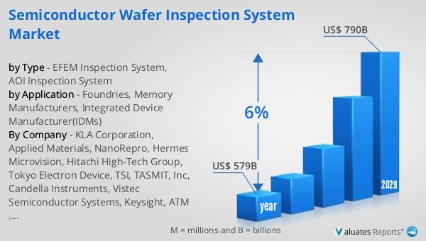
The global semiconductor market was valued at approximately $579 billion in 2022 and is anticipated to reach around $790 billion by 2029, reflecting a compound annual growth rate (CAGR) of 6% over the forecast period. This growth trajectory underscores the increasing demand for semiconductors across various industries, driven by advancements in technology and the proliferation of electronic devices. The semiconductor industry is a cornerstone of modern technology, providing the essential components for a wide range of applications, from consumer electronics to automotive systems and telecommunications infrastructure. As the world becomes more interconnected and reliant on digital technologies, the demand for semiconductors is expected to continue its upward trend. The projected growth of the semiconductor market highlights the importance of innovation and investment in research and development. Companies within the industry are continually striving to enhance the performance and efficiency of semiconductor devices, while also reducing costs and improving sustainability. This focus on innovation is crucial in meeting the evolving needs of consumers and businesses, as well as addressing the challenges posed by an increasingly competitive global market. Furthermore, the growth of the semiconductor market is likely to have a ripple effect on related industries, such as semiconductor equipment and materials. As demand for semiconductors increases, so too does the need for advanced manufacturing equipment and high-quality materials. This creates opportunities for companies operating in these sectors to capitalize on the growth of the semiconductor industry and expand their market presence. In conclusion, the global semiconductor market is poised for significant growth in the coming years, driven by technological advancements and increasing demand for electronic devices. This growth presents both challenges and opportunities for companies within the industry, as they navigate an ever-changing landscape and strive to meet the needs of a rapidly evolving market.
| Report Metric | Details |
| Report Name | Semiconductor Wafer Inspection System Market |
| Accounted market size in year | US$ 579 billion |
| Forecasted market size in 2029 | US$ 790 billion |
| CAGR | 6% |
| Base Year | year |
| Forecasted years | 2025 - 2029 |
| by Type |
|
| by Application |
|
| Production by Region |
|
| Consumption by Region |
|
| By Company | KLA Corporation, Applied Materials, NanoRepro, Hermes Microvision, Hitachi High-Tech Group, Tokyo Electron Device, TSI, TASMIT, Inc, Candella Instruments, Vistec Semiconductor Systems, Keysight, ATM Group, Cognex Corporation, Hanmi Semiconductor, MTI Instruments, Shanghai RSIC Scientific Instrument, Shenzhen Skyverse Technology, MegaRobo Technologies, Shenzhen Geling Jingrui Vision, Dongguan Ruizhi Photoelectric Technology, Teledyne DALSA, Nikon Precision, Newport Corporation, Nidec |
| Forecast units | USD million in value |
| Report coverage | Revenue and volume forecast, company share, competitive landscape, growth factors and trends |


