What is Global Semiconductor Wafer Frame Market?
The Global Semiconductor Wafer Frame Market is a crucial segment within the semiconductor industry, focusing on the production and supply of wafer frames used in semiconductor manufacturing. Wafer frames are essential components that hold semiconductor wafers during various stages of the manufacturing process, ensuring stability and precision. These frames are typically made from materials like stainless steel or aluminum, designed to withstand the rigorous conditions of semiconductor fabrication. The market for semiconductor wafer frames is driven by the increasing demand for semiconductors across various industries, including consumer electronics, automotive, and telecommunications. As technology advances, the need for more sophisticated and efficient semiconductor devices grows, further propelling the demand for high-quality wafer frames. The market is characterized by continuous innovation, with manufacturers striving to develop frames that offer enhanced performance, durability, and compatibility with advanced semiconductor manufacturing processes. Additionally, the global nature of the semiconductor industry means that the wafer frame market is influenced by international trade dynamics, technological advancements, and regional manufacturing capabilities. Overall, the Global Semiconductor Wafer Frame Market plays a vital role in supporting the semiconductor industry's growth and technological progress.
6 Inch, 8 Inch, 12 Inch, Others in the Global Semiconductor Wafer Frame Market:
In the Global Semiconductor Wafer Frame Market, wafer frames are categorized based on the size of the wafers they accommodate, with common sizes being 6-inch, 8-inch, and 12-inch, among others. Each size serves specific applications and is chosen based on the requirements of the semiconductor manufacturing process. The 6-inch wafer frames are typically used in older semiconductor manufacturing facilities or for specialized applications where smaller wafers are sufficient. These frames are often employed in the production of legacy semiconductor devices or in niche markets where the demand for smaller wafers persists. Despite the industry's shift towards larger wafer sizes, 6-inch frames remain relevant due to their cost-effectiveness and suitability for certain applications. On the other hand, 8-inch wafer frames represent a more widely used standard in the semiconductor industry. They offer a balance between cost and performance, making them suitable for a broad range of applications. The 8-inch size is often used in the production of various semiconductor devices, including microcontrollers, sensors, and power management chips. As the industry continues to evolve, 8-inch wafer frames remain a popular choice for many manufacturers due to their versatility and established infrastructure. The 12-inch wafer frames, however, represent the cutting edge of semiconductor manufacturing. These larger frames are used in the production of advanced semiconductor devices, such as microprocessors and memory chips, which require larger wafers to accommodate more complex circuitry. The shift towards 12-inch wafers is driven by the need for increased production efficiency and the ability to produce more chips per wafer. This transition is supported by advancements in manufacturing technology, which enable the production of larger wafers with higher yields. While the initial investment in 12-inch wafer manufacturing facilities is significant, the long-term benefits in terms of cost savings and production capacity make it an attractive option for leading semiconductor manufacturers. Beyond these standard sizes, the market also accommodates other wafer frame sizes, catering to specific applications and emerging technologies. These may include frames for experimental or custom wafer sizes used in research and development or specialized manufacturing processes. The diversity in wafer frame sizes reflects the dynamic nature of the semiconductor industry, where innovation and adaptation are key to meeting the evolving demands of technology and consumer markets. As the Global Semiconductor Wafer Frame Market continues to grow, the interplay between different wafer sizes and their respective applications will remain a critical factor in shaping the industry's future.
Wafer Dicing, Wafer Back Grinding, Wafer Sorting, Others in the Global Semiconductor Wafer Frame Market:
The Global Semiconductor Wafer Frame Market finds its applications in several critical areas of semiconductor manufacturing, including wafer dicing, wafer back grinding, wafer sorting, and others. Each of these processes plays a vital role in transforming raw semiconductor wafers into functional electronic components. Wafer dicing is the process of cutting a semiconductor wafer into individual chips or dies. This step is crucial as it determines the final size and shape of the semiconductor devices. Wafer frames are essential during dicing as they provide the necessary support and stability to the wafer, ensuring precise and clean cuts. The frames help prevent damage to the wafer and maintain the integrity of the individual chips, which is vital for their performance and reliability. In wafer back grinding, the thickness of the semiconductor wafer is reduced to meet the specifications required for packaging and assembly. This process is essential for creating thinner and lighter semiconductor devices, which are in high demand in the consumer electronics market. Wafer frames play a crucial role in back grinding by securely holding the wafer in place, preventing any movement or vibration that could lead to damage or defects. The frames ensure that the grinding process is uniform and consistent, resulting in high-quality wafers ready for further processing. Wafer sorting is another critical application of wafer frames, where individual chips are tested and categorized based on their performance and quality. This process involves handling and inspecting each chip to ensure it meets the required standards before packaging. Wafer frames facilitate the sorting process by providing a stable platform for the wafers, allowing for efficient and accurate testing. The frames help minimize handling errors and reduce the risk of damage to the delicate semiconductor chips. Beyond these specific applications, wafer frames are also used in other stages of semiconductor manufacturing, such as wafer cleaning, inspection, and packaging. In each of these processes, the frames provide the necessary support and protection to the wafers, ensuring that they remain intact and free from contamination. The versatility and reliability of wafer frames make them indispensable in the semiconductor manufacturing process, contributing to the production of high-quality and high-performance electronic components. As the demand for advanced semiconductor devices continues to grow, the role of wafer frames in supporting these critical manufacturing processes will remain essential.
Global Semiconductor Wafer Frame Market Outlook:
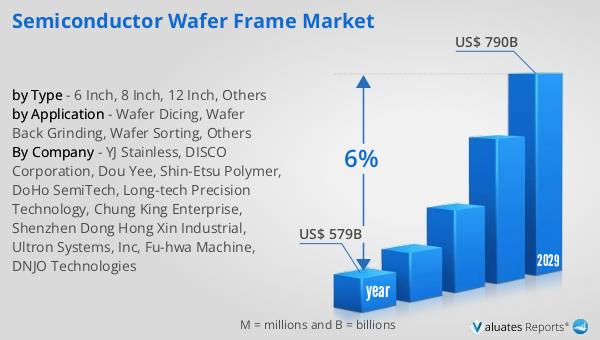
In 2022, the global semiconductor market was valued at approximately $579 billion. This figure highlights the immense scale and significance of the semiconductor industry in the global economy. Looking ahead, projections indicate that the market is set to grow to around $790 billion by 2029. This anticipated growth represents a compound annual growth rate (CAGR) of 6% over the forecast period. Such growth is indicative of the increasing demand for semiconductors across various sectors, including consumer electronics, automotive, telecommunications, and more. The expansion of the semiconductor market is driven by several factors, including technological advancements, the proliferation of connected devices, and the ongoing digital transformation across industries. As the world becomes more reliant on technology, the need for semiconductors, which are the building blocks of modern electronic devices, continues to rise. This growth trajectory underscores the importance of the semiconductor industry in driving innovation and supporting the development of new technologies. The projected increase in market value also reflects the industry's ability to adapt to changing market dynamics and meet the evolving needs of consumers and businesses. As the semiconductor market continues to expand, it will play a crucial role in shaping the future of technology and driving economic growth on a global scale.
| Report Metric | Details |
| Report Name | Semiconductor Wafer Frame Market |
| Accounted market size in year | US$ 579 billion |
| Forecasted market size in 2029 | US$ 790 billion |
| CAGR | 6% |
| Base Year | year |
| Forecasted years | 2025 - 2029 |
| by Type |
|
| by Application |
|
| Production by Region |
|
| Consumption by Region |
|
| By Company | YJ Stainless, DISCO Corporation, Dou Yee, Shin-Etsu Polymer, DoHo SemiTech, Long-tech Precision Technology, Chung King Enterprise, Shenzhen Dong Hong Xin Industrial, Ultron Systems, Inc, Fu-hwa Machine, DNJO Technologies |
| Forecast units | USD million in value |
| Report coverage | Revenue and volume forecast, company share, competitive landscape, growth factors and trends |


