What is Global Semiconductor Optical Critical Dimension (OCD) Metrology Equipment Market?
The Global Semiconductor Optical Critical Dimension (OCD) Metrology Equipment Market is a specialized segment within the semiconductor industry that focuses on the precise measurement of the critical dimensions of semiconductor devices. These measurements are crucial for ensuring the performance and reliability of semiconductor components, which are integral to a wide range of electronic devices. OCD metrology equipment utilizes advanced optical techniques to measure the dimensions of semiconductor features at the nanometer scale. This market is driven by the increasing demand for smaller, more powerful, and energy-efficient electronic devices, which require precise control over the manufacturing process. As semiconductor technology continues to advance, the need for accurate and reliable metrology solutions becomes even more critical. The market encompasses various types of equipment, including ellipsometers and spectroscopic reflectometers, which are used to measure different aspects of semiconductor devices. The growth of this market is supported by ongoing research and development efforts aimed at improving the accuracy and efficiency of OCD metrology equipment. As a result, the Global Semiconductor OCD Metrology Equipment Market plays a vital role in the advancement of semiconductor technology and the broader electronics industry.
Ellipsometer, Spectroscopic Reflectometer in the Global Semiconductor Optical Critical Dimension (OCD) Metrology Equipment Market:
Ellipsometers and spectroscopic reflectometers are two key types of equipment used in the Global Semiconductor Optical Critical Dimension (OCD) Metrology Equipment Market. Ellipsometers are optical instruments that measure the change in polarization as light reflects or transmits through a sample. They are widely used in the semiconductor industry to determine the thickness and optical properties of thin films. By analyzing the change in polarization, ellipsometers can provide precise measurements of film thickness, refractive index, and extinction coefficient. This information is crucial for controlling the manufacturing process and ensuring the quality of semiconductor devices. Spectroscopic reflectometers, on the other hand, measure the intensity of light reflected from a sample as a function of wavelength. This technique is used to determine the thickness and optical properties of thin films, as well as the critical dimensions of semiconductor features. Spectroscopic reflectometers are particularly useful for measuring complex multilayer structures, which are common in advanced semiconductor devices. Both ellipsometers and spectroscopic reflectometers are essential tools in the semiconductor industry, providing the precise measurements needed to ensure the performance and reliability of semiconductor devices. The demand for these instruments is driven by the increasing complexity of semiconductor devices and the need for precise control over the manufacturing process. As semiconductor technology continues to advance, the capabilities of ellipsometers and spectroscopic reflectometers are also evolving, with ongoing research and development efforts aimed at improving their accuracy and efficiency. These advancements are critical for meeting the demands of the semiconductor industry and supporting the development of next-generation electronic devices. The Global Semiconductor OCD Metrology Equipment Market is characterized by a high level of innovation, with manufacturers continually developing new and improved metrology solutions to meet the needs of the industry. This dynamic market is driven by the rapid pace of technological change in the semiconductor industry, as well as the increasing demand for smaller, more powerful, and energy-efficient electronic devices. As a result, ellipsometers and spectroscopic reflectometers play a vital role in the advancement of semiconductor technology and the broader electronics industry.
200 mm Wafer, Others in the Global Semiconductor Optical Critical Dimension (OCD) Metrology Equipment Market:
The Global Semiconductor Optical Critical Dimension (OCD) Metrology Equipment Market plays a crucial role in the production and quality assurance of semiconductor wafers, including 200 mm wafers and other types. In the context of 200 mm wafers, OCD metrology equipment is used to measure the critical dimensions of semiconductor features with high precision. This is essential for ensuring the performance and reliability of semiconductor devices, as even small deviations in dimensions can significantly impact the functionality of the final product. The use of OCD metrology equipment in the production of 200 mm wafers helps manufacturers maintain tight control over the manufacturing process, reducing the risk of defects and improving yield. This is particularly important in the semiconductor industry, where the cost of defects can be extremely high. In addition to 200 mm wafers, OCD metrology equipment is also used in the production of other types of semiconductor wafers, including 300 mm wafers and advanced node technologies. These applications require even greater precision and accuracy, as the features on these wafers are often smaller and more complex. The ability to accurately measure these features is critical for ensuring the performance and reliability of the final product. The Global Semiconductor OCD Metrology Equipment Market is characterized by a high level of innovation, with manufacturers continually developing new and improved metrology solutions to meet the needs of the industry. This dynamic market is driven by the rapid pace of technological change in the semiconductor industry, as well as the increasing demand for smaller, more powerful, and energy-efficient electronic devices. As a result, OCD metrology equipment plays a vital role in the advancement of semiconductor technology and the broader electronics industry. The use of OCD metrology equipment in the production of semiconductor wafers is essential for ensuring the quality and performance of the final product. By providing precise measurements of critical dimensions, these instruments help manufacturers maintain tight control over the manufacturing process, reducing the risk of defects and improving yield. This is particularly important in the semiconductor industry, where the cost of defects can be extremely high. As semiconductor technology continues to advance, the capabilities of OCD metrology equipment are also evolving, with ongoing research and development efforts aimed at improving their accuracy and efficiency. These advancements are critical for meeting the demands of the semiconductor industry and supporting the development of next-generation electronic devices.
Global Semiconductor Optical Critical Dimension (OCD) Metrology Equipment Market Outlook:
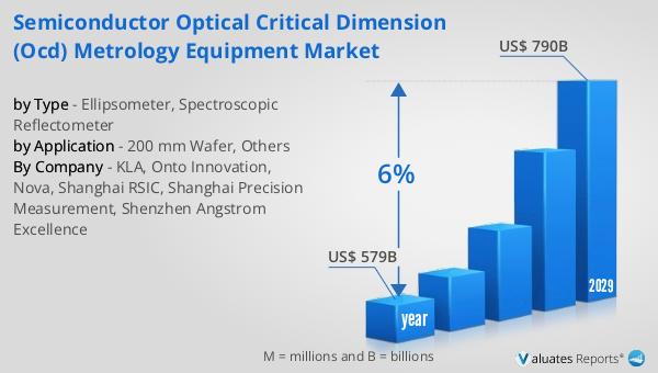
The global semiconductor market was valued at approximately $579 billion in 2022 and is anticipated to reach around $790 billion by 2029, reflecting a compound annual growth rate (CAGR) of 6% over the forecast period. This growth trajectory underscores the increasing demand for semiconductors, driven by advancements in technology and the proliferation of electronic devices across various sectors. The semiconductor industry is pivotal to the functioning of modern technology, serving as the backbone for a wide array of applications, from consumer electronics to industrial machinery. The projected growth in the semiconductor market is indicative of the ongoing innovation and development within the industry, as manufacturers strive to meet the evolving needs of consumers and businesses alike. The expansion of the semiconductor market is also fueled by the growing adoption of technologies such as artificial intelligence, the Internet of Things (IoT), and 5G, which require advanced semiconductor solutions to function effectively. As the demand for these technologies continues to rise, the semiconductor industry is poised for significant growth, with companies investing heavily in research and development to stay competitive. The anticipated increase in market value reflects the critical role that semiconductors play in enabling technological progress and driving economic growth. As the industry continues to evolve, the global semiconductor market is expected to remain a key driver of innovation and development, supporting the advancement of technology and the broader economy.
| Report Metric | Details |
| Report Name | Semiconductor Optical Critical Dimension (OCD) Metrology Equipment Market |
| Accounted market size in year | US$ 579 billion |
| Forecasted market size in 2029 | US$ 790 billion |
| CAGR | 6% |
| Base Year | year |
| Forecasted years | 2025 - 2029 |
| by Type |
|
| by Application |
|
| Production by Region |
|
| Consumption by Region |
|
| By Company | KLA, Onto Innovation, Nova, Shanghai RSIC, Shanghai Precision Measurement, Shenzhen Angstrom Excellence |
| Forecast units | USD million in value |
| Report coverage | Revenue and volume forecast, company share, competitive landscape, growth factors and trends |