What is Global Semiconductor Metrology and Inspection Systems Market?
The Global Semiconductor Metrology and Inspection Systems Market is a crucial segment of the semiconductor industry, focusing on the tools and technologies used to measure and inspect semiconductor devices. These systems are essential for ensuring the quality and performance of semiconductors, which are integral components in a wide range of electronic devices. The market encompasses various types of equipment, including defect inspection systems and metrology systems, which are used to detect and measure defects and variations in semiconductor wafers and other components. As the demand for smaller, more powerful, and efficient electronic devices continues to grow, the need for advanced metrology and inspection systems becomes increasingly important. These systems help manufacturers maintain high standards of quality and reliability, which are critical for the success of semiconductor products in the global market. The market is driven by technological advancements, increasing complexity of semiconductor devices, and the need for precise measurement and inspection solutions. As a result, the Global Semiconductor Metrology and Inspection Systems Market is expected to experience significant growth in the coming years, driven by the ongoing evolution of the semiconductor industry and the increasing demand for high-quality electronic devices.
Defect Inspection Systems, Metrology Systems in the Global Semiconductor Metrology and Inspection Systems Market:
Defect inspection systems and metrology systems are two key components of the Global Semiconductor Metrology and Inspection Systems Market. Defect inspection systems are designed to identify and analyze defects in semiconductor wafers and other components. These systems use advanced imaging and detection technologies to locate and classify defects, such as particles, scratches, and pattern deviations, which can affect the performance and reliability of semiconductor devices. By identifying defects early in the manufacturing process, these systems help manufacturers improve yield and reduce production costs. Metrology systems, on the other hand, are used to measure the physical and electrical properties of semiconductor devices. These systems provide precise measurements of critical dimensions, such as line width, thickness, and overlay, which are essential for ensuring the performance and functionality of semiconductor devices. Metrology systems use a variety of techniques, including optical, electron beam, and X-ray metrology, to achieve high levels of accuracy and precision. The integration of defect inspection and metrology systems is crucial for maintaining the quality and reliability of semiconductor devices, as they provide comprehensive data and insights into the manufacturing process. As semiconductor devices become more complex and miniaturized, the demand for advanced defect inspection and metrology systems continues to grow. Manufacturers are increasingly investing in these systems to enhance their production capabilities and meet the stringent quality standards required by the industry. The development of new technologies, such as artificial intelligence and machine learning, is also driving innovation in the field of semiconductor metrology and inspection, enabling more efficient and accurate defect detection and measurement. As a result, the Global Semiconductor Metrology and Inspection Systems Market is poised for significant growth, driven by the increasing demand for high-quality semiconductor devices and the need for advanced measurement and inspection solutions.
Wafer, Mask/Film, Other in the Global Semiconductor Metrology and Inspection Systems Market:
The usage of Global Semiconductor Metrology and Inspection Systems Market extends to various areas, including wafer, mask/film, and other components. In the wafer segment, metrology and inspection systems are used to ensure the quality and performance of semiconductor wafers, which are the foundational building blocks of semiconductor devices. These systems help manufacturers detect and analyze defects, measure critical dimensions, and ensure the uniformity and consistency of wafers. By providing accurate and reliable data, metrology and inspection systems enable manufacturers to optimize their production processes and improve yield. In the mask/film segment, these systems are used to inspect and measure photomasks and films, which are essential for the photolithography process in semiconductor manufacturing. Photomasks are used to transfer circuit patterns onto semiconductor wafers, and any defects or variations in the masks can lead to defects in the final semiconductor devices. Metrology and inspection systems help manufacturers ensure the quality and accuracy of photomasks and films, reducing the risk of defects and improving the overall quality of semiconductor devices. In addition to wafers and masks/films, metrology and inspection systems are also used in other areas of semiconductor manufacturing, such as packaging and assembly. These systems help manufacturers ensure the quality and reliability of semiconductor packages, which protect and connect semiconductor devices to other components. By providing comprehensive data and insights into the manufacturing process, metrology and inspection systems enable manufacturers to maintain high standards of quality and reliability, which are critical for the success of semiconductor products in the global market. As the demand for smaller, more powerful, and efficient electronic devices continues to grow, the need for advanced metrology and inspection systems becomes increasingly important, driving the growth of the Global Semiconductor Metrology and Inspection Systems Market.
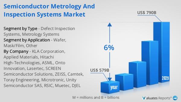
Global Semiconductor Metrology and Inspection Systems Market Outlook:
The global market for semiconductors was valued at approximately $579 billion in 2022 and is anticipated to reach around $790 billion by 2029, reflecting a compound annual growth rate (CAGR) of 6% over the forecast period. This growth trajectory underscores the increasing demand for semiconductors across various industries, driven by technological advancements and the proliferation of electronic devices. The semiconductor industry plays a pivotal role in the global economy, as semiconductors are essential components in a wide range of products, from consumer electronics to industrial machinery. The projected growth in the semiconductor market is fueled by several factors, including the rising demand for high-performance computing, the expansion of the Internet of Things (IoT), and the increasing adoption of artificial intelligence and machine learning technologies. As the demand for more powerful and efficient electronic devices continues to rise, the semiconductor industry is poised for significant growth, with manufacturers investing in advanced technologies and production capabilities to meet the evolving needs of the market. The Global Semiconductor Metrology and Inspection Systems Market is an integral part of this growth, as it provides the tools and technologies necessary to ensure the quality and performance of semiconductor devices. By enabling manufacturers to maintain high standards of quality and reliability, metrology and inspection systems play a crucial role in supporting the growth and success of the semiconductor industry.
| Report Metric | Details |
| Report Name | Semiconductor Metrology and Inspection Systems Market |
| Accounted market size in year | US$ 579 billion |
| Forecasted market size in 2029 | US$ 790 billion |
| CAGR | 6% |
| Base Year | year |
| Forecasted years | 2025 - 2029 |
| Segment by Type |
|
| Segment by Application |
|
| By Region |
|
| By Company | KLA Corporation, Applied Materials, Hitachi High-Technologies, ASML, Onto Innovation, Lasertec, SCREEN Semiconductor Solutions, ZEISS, Camtek, Toray Engineering, Microtronic, Unity Semiconductor SAS, RSIC, Muetec, DJEL |
| Forecast units | USD million in value |
| Report coverage | Revenue and volume forecast, company share, competitive landscape, growth factors and trends |


