What is Global Semiconductor Inspection and Measurement Systems Market?
The Global Semiconductor Inspection and Measurement Systems Market is a crucial segment within the broader semiconductor industry, focusing on ensuring the quality and precision of semiconductor devices. These systems are essential for maintaining the integrity and performance of semiconductors, which are the building blocks of modern electronics. The market encompasses a range of technologies and solutions designed to inspect and measure semiconductor wafers, masks, and other components during the manufacturing process. As the demand for smaller, faster, and more efficient electronic devices grows, the need for advanced inspection and measurement systems becomes increasingly important. These systems help manufacturers detect defects, ensure compliance with stringent industry standards, and optimize production processes. The market is driven by technological advancements, increasing complexity of semiconductor devices, and the need for high-quality assurance in the production of integrated circuits. With the semiconductor industry continuously evolving, the inspection and measurement systems market plays a vital role in supporting innovation and maintaining competitive advantage. As a result, companies in this market are investing in research and development to offer cutting-edge solutions that meet the ever-changing demands of the semiconductor industry.
Defect Inspection Systems, Metrology Systems in the Global Semiconductor Inspection and Measurement Systems Market:
Defect inspection systems and metrology systems are two critical components of the Global Semiconductor Inspection and Measurement Systems Market. Defect inspection systems are designed to identify and analyze defects on semiconductor wafers and masks. These systems use advanced imaging technologies, such as optical and electron microscopy, to detect surface and subsurface defects that can affect the performance and reliability of semiconductor devices. By identifying defects early in the manufacturing process, these systems help manufacturers reduce waste, improve yield, and ensure the quality of their products. Metrology systems, on the other hand, focus on measuring the physical dimensions and properties of semiconductor devices. These systems use techniques such as scanning electron microscopy (SEM), atomic force microscopy (AFM), and optical metrology to provide precise measurements of critical dimensions, film thickness, and other parameters. Accurate metrology is essential for ensuring that semiconductor devices meet design specifications and function as intended. Both defect inspection and metrology systems are integral to the semiconductor manufacturing process, as they provide the data and insights needed to optimize production and maintain high standards of quality. As semiconductor devices become more complex and feature smaller geometries, the demand for advanced inspection and metrology solutions continues to grow. Manufacturers are increasingly relying on these systems to address the challenges of producing next-generation semiconductors, which require higher levels of precision and accuracy. The integration of artificial intelligence and machine learning technologies into inspection and metrology systems is also enhancing their capabilities, enabling faster and more accurate analysis of semiconductor devices. This technological evolution is helping manufacturers improve their processes, reduce costs, and accelerate time-to-market for new products. In summary, defect inspection and metrology systems are essential tools in the semiconductor industry, providing the necessary support for quality assurance and process optimization. As the industry continues to advance, these systems will play an increasingly important role in enabling the production of innovative and high-performance semiconductor devices.
Wafer, Mask/Film, Other in the Global Semiconductor Inspection and Measurement Systems Market:
The usage of Global Semiconductor Inspection and Measurement Systems Market extends across various areas, including wafers, masks/films, and other components. In the context of wafers, these systems are employed to inspect and measure the quality and dimensions of semiconductor wafers, which are the foundational substrates for integrated circuits. Wafers undergo multiple processing steps, and inspection systems are used at various stages to detect defects such as scratches, particles, and pattern deviations. Metrology systems measure critical dimensions, film thickness, and other parameters to ensure that the wafers meet design specifications. This is crucial for maintaining the performance and reliability of the final semiconductor devices. In the area of masks and films, inspection and measurement systems play a vital role in ensuring the accuracy and precision of photomasks, which are used in the photolithography process to transfer circuit patterns onto wafers. Defects in masks can lead to errors in the patterning process, affecting the yield and performance of semiconductor devices. Inspection systems detect defects such as pinholes, contamination, and pattern misalignments, while metrology systems measure critical dimensions and overlay accuracy. This ensures that the masks and films used in semiconductor manufacturing are of the highest quality, minimizing the risk of defects in the final products. Beyond wafers and masks, inspection and measurement systems are also used in other areas of semiconductor manufacturing, such as packaging and assembly. These systems help ensure the quality and reliability of semiconductor packages, which protect and connect the integrated circuits to the external environment. Inspection systems detect defects such as delamination, voids, and misalignments, while metrology systems measure critical dimensions and other parameters to ensure that the packages meet industry standards. Overall, the usage of inspection and measurement systems in these areas is essential for maintaining the quality and performance of semiconductor devices, supporting the industry's drive for innovation and excellence.
Global Semiconductor Inspection and Measurement Systems Market Outlook:
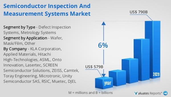
The global semiconductor market, valued at approximately $579 billion in 2022, is on a growth trajectory, with projections indicating it will reach around $790 billion by 2029. This growth represents a compound annual growth rate (CAGR) of 6% over the forecast period. This expansion is driven by the increasing demand for semiconductors across various industries, including consumer electronics, automotive, telecommunications, and healthcare. As technology continues to advance, the need for more powerful and efficient semiconductor devices is growing, fueling the demand for inspection and measurement systems that ensure the quality and reliability of these components. The semiconductor industry is characterized by rapid innovation and the continuous development of new technologies, which require precise and accurate inspection and measurement solutions. As a result, the Global Semiconductor Inspection and Measurement Systems Market is expected to play a crucial role in supporting the industry's growth by providing the necessary tools and technologies to maintain high standards of quality and performance. Companies in this market are investing in research and development to offer advanced solutions that meet the evolving needs of the semiconductor industry, ensuring that they remain competitive in a rapidly changing landscape. This growth in the semiconductor market underscores the importance of inspection and measurement systems in enabling the production of high-quality semiconductor devices that power the technologies of the future.
| Report Metric | Details |
| Report Name | Semiconductor Inspection and Measurement Systems Market |
| Accounted market size in year | US$ 579 billion |
| Forecasted market size in 2029 | US$ 790 billion |
| CAGR | 6% |
| Base Year | year |
| Forecasted years | 2025 - 2029 |
| Segment by Type |
|
| Segment by Application |
|
| By Region |
|
| By Company | KLA Corporation, Applied Materials, Hitachi High-Technologies, ASML, Onto Innovation, Lasertec, SCREEN Semiconductor Solutions, ZEISS, Camtek, Toray Engineering, Microtronic, Unity Semiconductor SAS, RSIC, Muetec, DJEL |
| Forecast units | USD million in value |
| Report coverage | Revenue and volume forecast, company share, competitive landscape, growth factors and trends |


