What is Global Semiconductor EUV Pellicles Market?
The Global Semiconductor EUV Pellicles Market is a specialized segment within the semiconductor industry that focuses on the production and application of pellicles used in extreme ultraviolet (EUV) lithography. EUV lithography is a cutting-edge technology employed in the manufacturing of semiconductors, enabling the creation of smaller and more powerful microchips. Pellicles are thin, transparent membranes that protect photomasks from contamination during the lithography process, ensuring the integrity and precision of the patterns transferred onto silicon wafers. The demand for EUV pellicles is driven by the semiconductor industry's relentless pursuit of miniaturization and enhanced performance, as they are crucial in achieving the high-resolution patterns required for advanced semiconductor devices. As technology nodes continue to shrink, the role of EUV pellicles becomes increasingly vital, making this market a key component in the broader semiconductor manufacturing ecosystem. The market is characterized by rapid technological advancements, with ongoing research and development efforts aimed at improving pellicle materials and designs to meet the stringent requirements of EUV lithography. This market's growth is closely tied to the overall expansion of the semiconductor industry, as it supports the production of next-generation electronic devices.
Above 90% Transmittance, ≤90% Transmittance in the Global Semiconductor EUV Pellicles Market:
In the Global Semiconductor EUV Pellicles Market, transmittance is a critical factor that determines the efficiency and effectiveness of pellicles used in EUV lithography. Transmittance refers to the percentage of EUV light that passes through the pellicle without being absorbed or reflected. Two primary categories of transmittance are considered: Above 90% Transmittance and ≤90% Transmittance. Pellicles with Above 90% Transmittance are designed to allow a higher percentage of EUV light to pass through, which is essential for achieving high-resolution patterning on semiconductor wafers. These pellicles are typically made from advanced materials that offer superior optical clarity and minimal absorption, ensuring that the maximum amount of EUV light reaches the photomask and subsequently the wafer. The high transmittance is crucial for maintaining the throughput and efficiency of the lithography process, as it reduces the need for increased exposure times and enhances the overall productivity of semiconductor manufacturing. On the other hand, pellicles with ≤90% Transmittance are designed for applications where slightly lower transmittance is acceptable or where cost considerations may dictate the use of less advanced materials. These pellicles still provide adequate protection for photomasks but may require adjustments in the lithography process to compensate for the reduced light transmission. The choice between Above 90% Transmittance and ≤90% Transmittance pellicles depends on various factors, including the specific requirements of the semiconductor manufacturing process, the desired resolution and throughput, and the cost constraints of the production environment. Manufacturers must carefully evaluate these factors to select the appropriate pellicle type that aligns with their production goals and technological capabilities. As the semiconductor industry continues to evolve, the demand for high-transmittance pellicles is expected to grow, driven by the need for more precise and efficient lithography processes. This trend underscores the importance of ongoing research and development efforts aimed at enhancing the transmittance properties of EUV pellicles, as well as the exploration of new materials and technologies that can further optimize their performance. The development of pellicles with even higher transmittance levels could unlock new possibilities for semiconductor manufacturing, enabling the production of increasingly complex and powerful electronic devices. In conclusion, the transmittance characteristics of EUV pellicles play a pivotal role in the Global Semiconductor EUV Pellicles Market, influencing the efficiency, resolution, and cost-effectiveness of the lithography process. As the industry continues to push the boundaries of semiconductor technology, the demand for high-performance pellicles with superior transmittance properties is likely to remain a key driver of market growth.
IDM, Foundry in the Global Semiconductor EUV Pellicles Market:
The usage of Global Semiconductor EUV Pellicles Market in Integrated Device Manufacturers (IDM) and Foundries is a critical aspect of the semiconductor manufacturing landscape. IDMs are companies that design, manufacture, and sell their own semiconductor products, while foundries are specialized facilities that manufacture semiconductors for other companies, often referred to as fabless companies. In both cases, EUV pellicles play a vital role in ensuring the quality and efficiency of the lithography process, which is central to semiconductor production. For IDMs, the use of EUV pellicles is integral to maintaining the integrity of their photomasks, which are used to transfer intricate circuit patterns onto silicon wafers. The high transmittance and protective properties of EUV pellicles help prevent contamination and defects, ensuring that the final semiconductor products meet the stringent quality standards required for various applications, from consumer electronics to automotive systems. By utilizing EUV pellicles, IDMs can achieve higher yields and reduce the risk of costly rework or product recalls, ultimately enhancing their competitiveness in the market. In foundries, the application of EUV pellicles is equally important, as these facilities often operate at high volumes and must meet the diverse needs of multiple clients. The use of pellicles with optimal transmittance properties allows foundries to deliver high-quality semiconductor products with precise patterning and minimal defects. This capability is crucial for attracting and retaining clients, as fabless companies rely on foundries to produce semiconductors that meet their specific design and performance requirements. Additionally, the use of EUV pellicles in foundries supports the efficient scaling of production processes, enabling these facilities to accommodate the growing demand for advanced semiconductor devices. The collaboration between IDMs, foundries, and pellicle manufacturers is essential for driving innovation and advancing the capabilities of EUV lithography. As the semiconductor industry continues to evolve, the need for more sophisticated and efficient pellicles will become increasingly pronounced, prompting ongoing research and development efforts to enhance their performance and cost-effectiveness. This collaborative approach ensures that both IDMs and foundries can leverage the latest advancements in pellicle technology to optimize their production processes and deliver cutting-edge semiconductor products to the market. In summary, the usage of Global Semiconductor EUV Pellicles Market in IDM and Foundry operations is a cornerstone of modern semiconductor manufacturing, enabling these entities to achieve high-quality, efficient, and cost-effective production outcomes. As the demand for advanced semiconductor devices continues to grow, the role of EUV pellicles in supporting the industry's technological advancements and competitive positioning will remain a critical focus for manufacturers and researchers alike.
Global Semiconductor EUV Pellicles Market Outlook:
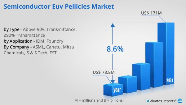
In 2024, the global market for Semiconductor EUV Pellicles was valued at approximately $78.8 million. This market is anticipated to experience significant growth over the coming years, with projections indicating that it will reach an estimated size of $171 million by 2031. This growth trajectory reflects a compound annual growth rate (CAGR) of 8.6% during the forecast period. The expansion of this market is driven by the increasing adoption of EUV lithography in semiconductor manufacturing, as the industry seeks to produce smaller, more powerful, and energy-efficient electronic devices. The demand for EUV pellicles is closely linked to the broader trends in the semiconductor industry, including the push for miniaturization and enhanced performance of microchips. As technology nodes continue to shrink, the precision and efficiency of the lithography process become paramount, underscoring the importance of high-quality pellicles. The projected growth of the Semiconductor EUV Pellicles Market highlights the critical role these components play in advancing semiconductor technology and supporting the production of next-generation electronic devices. This market's expansion is also indicative of the ongoing research and development efforts aimed at improving pellicle materials and designs to meet the evolving needs of the semiconductor industry. As manufacturers continue to innovate and refine their production processes, the demand for advanced EUV pellicles is expected to remain robust, driving further growth and development in this specialized market segment.
| Report Metric | Details |
| Report Name | Semiconductor EUV Pellicles Market |
| Accounted market size in year | US$ 78.8 million |
| Forecasted market size in 2031 | US$ 171 million |
| CAGR | 8.6% |
| Base Year | year |
| Forecasted years | 2025 - 2031 |
| by Type |
|
| by Application |
|
| Production by Region |
|
| Consumption by Region |
|
| By Company | ASML, Canatu, Mitsui Chemicals, S & S Tech, FST |
| Forecast units | USD million in value |
| Report coverage | Revenue and volume forecast, company share, competitive landscape, growth factors and trends |


