What is Global EUV Pellicle Market?
The Global EUV Pellicle Market is a specialized segment within the semiconductor industry, focusing on the development and production of pellicles used in extreme ultraviolet (EUV) lithography. EUV lithography is a cutting-edge technology employed in the manufacturing of semiconductors, enabling the production of smaller and more powerful microchips. Pellicles are thin, transparent membranes that protect photomasks from contamination during the lithography process, ensuring high yields and efficiency. The demand for EUV pellicles has been growing due to the increasing complexity and miniaturization of semiconductor devices. As the semiconductor industry continues to push the boundaries of Moore's Law, the need for advanced lithography techniques like EUV becomes more critical. The global market for EUV pellicles is driven by the rapid advancements in technology, the rising demand for consumer electronics, and the expansion of data centers and cloud computing. Companies in this market are investing heavily in research and development to improve pellicle materials and enhance their transmittance and durability. The market is characterized by intense competition, with key players striving to develop innovative solutions to meet the evolving needs of the semiconductor industry.
≥90% transmittance, <90% transmittance in the Global EUV Pellicle Market:
In the Global EUV Pellicle Market, transmittance is a crucial factor that determines the efficiency and effectiveness of pellicles used in EUV lithography. Transmittance refers to the ability of the pellicle to allow EUV light to pass through it without significant loss. Pellicles with ≥90% transmittance are highly sought after because they enable more light to reach the photomask, resulting in better image quality and higher throughput in the lithography process. These high-transmittance pellicles are essential for advanced semiconductor manufacturing, where precision and efficiency are paramount. The development of pellicles with ≥90% transmittance involves advanced materials and manufacturing techniques to ensure minimal absorption and scattering of EUV light. Companies in the EUV pellicle market are investing in research and development to achieve this high level of transmittance, as it directly impacts the performance and cost-effectiveness of semiconductor production. On the other hand, pellicles with <90% transmittance are also used in certain applications, although they may not offer the same level of efficiency as their higher-transmittance counterparts. These pellicles are typically employed in less demanding lithography processes or where cost considerations are a priority. The choice between ≥90% and <90% transmittance pellicles depends on the specific requirements of the semiconductor manufacturing process, including factors such as the complexity of the design, production volume, and cost constraints. As the semiconductor industry continues to evolve, the demand for high-transmittance pellicles is expected to increase, driven by the need for more advanced and efficient manufacturing processes. Companies in the EUV pellicle market are focusing on developing innovative solutions to meet this demand, including the use of new materials and technologies to enhance transmittance and durability. The competition in the market is intense, with key players striving to gain a competitive edge by offering pellicles with superior performance and reliability. The development of pellicles with ≥90% transmittance is a complex and challenging process, requiring significant investment in research and development. Companies are exploring various approaches to achieve this goal, including the use of advanced materials such as silicon, carbon, and other high-performance polymers. These materials are designed to minimize absorption and scattering of EUV light, ensuring maximum transmittance and optimal performance in the lithography process. In addition to materials, manufacturing techniques also play a crucial role in achieving high transmittance. Advanced fabrication methods, such as atomic layer deposition and chemical vapor deposition, are used to create thin, uniform pellicle films with precise control over thickness and composition. These techniques help to minimize defects and ensure consistent performance across the entire pellicle surface. The development of pellicles with ≥90% transmittance is not only a technical challenge but also a strategic priority for companies in the EUV pellicle market. As the demand for more advanced and efficient semiconductor manufacturing processes continues to grow, the ability to offer high-transmittance pellicles will be a key differentiator for companies in this competitive market. By investing in research and development and leveraging advanced materials and manufacturing techniques, companies can position themselves as leaders in the EUV pellicle market and capitalize on the growing demand for high-performance pellicles.
IDM, Foundry in the Global EUV Pellicle Market:
The usage of Global EUV Pellicle Market in areas such as Integrated Device Manufacturers (IDM) and Foundries is crucial for the advancement of semiconductor technology. IDMs are companies that design, manufacture, and sell integrated circuits (ICs) and other semiconductor devices. They rely heavily on EUV lithography to produce cutting-edge chips with smaller nodes and higher performance. The use of EUV pellicles in IDM operations ensures that the photomasks used in the lithography process are protected from contamination, leading to higher yields and reduced production costs. By incorporating high-transmittance pellicles, IDMs can achieve better image quality and throughput, which are essential for maintaining competitiveness in the semiconductor market. Foundries, on the other hand, are companies that specialize in manufacturing semiconductor devices for other companies. They play a critical role in the semiconductor supply chain, providing manufacturing services to fabless companies and other IDMs. Foundries utilize EUV lithography to produce a wide range of semiconductor products, from microprocessors to memory chips. The use of EUV pellicles in foundry operations is vital for ensuring the quality and reliability of the chips produced. High-transmittance pellicles enable foundries to achieve the precision and efficiency required for advanced semiconductor manufacturing, allowing them to meet the demands of their customers. The integration of EUV pellicles in both IDM and foundry operations is driven by the need for more advanced and efficient manufacturing processes. As the semiconductor industry continues to evolve, the demand for smaller, faster, and more energy-efficient chips is increasing. This trend is pushing IDMs and foundries to adopt EUV lithography and invest in high-performance pellicles to stay competitive. The use of EUV pellicles in these areas is not only a technical necessity but also a strategic advantage, enabling companies to produce cutting-edge semiconductor devices that meet the demands of the modern market. The collaboration between pellicle manufacturers and semiconductor companies is essential for the successful integration of EUV pellicles in IDM and foundry operations. By working closely with their customers, pellicle manufacturers can develop customized solutions that meet the specific needs of each company, ensuring optimal performance and cost-effectiveness. This collaboration is crucial for driving innovation and advancing the capabilities of EUV lithography, ultimately benefiting the entire semiconductor industry. As the demand for more advanced semiconductor devices continues to grow, the role of EUV pellicles in IDM and foundry operations will become increasingly important. Companies that can offer high-performance pellicles with superior transmittance and durability will be well-positioned to capitalize on this growing market and drive the future of semiconductor manufacturing.
Global EUV Pellicle Market Outlook:
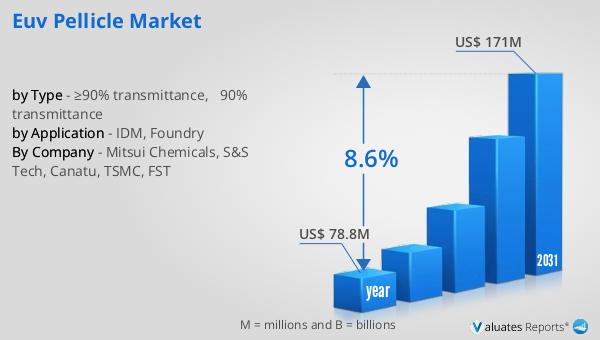
The global market for EUV pellicles was valued at approximately $78.8 million in 2024, with projections indicating a significant growth trajectory. By 2031, the market is expected to reach an estimated size of $171 million, reflecting a compound annual growth rate (CAGR) of 8.6% over the forecast period. This growth is driven by the increasing adoption of EUV lithography in semiconductor manufacturing, as companies strive to produce smaller and more powerful microchips. In 2021, a notable development in the market was the introduction of a pellicle with transmittance exceeding 90% by the South Korean company SS Tech. This advancement highlights the ongoing efforts by industry players to enhance pellicle performance and meet the evolving demands of the semiconductor industry. The development of high-transmittance pellicles is a critical factor in the market's growth, as it directly impacts the efficiency and effectiveness of EUV lithography processes. Companies are investing in research and development to improve pellicle materials and manufacturing techniques, ensuring that they can offer products that meet the stringent requirements of modern semiconductor manufacturing. The competition in the EUV pellicle market is intense, with key players striving to gain a competitive edge by offering innovative solutions that enhance transmittance and durability. As the market continues to expand, companies that can deliver high-performance pellicles will be well-positioned to capitalize on the growing demand for advanced semiconductor manufacturing technologies.
| Report Metric | Details |
| Report Name | EUV Pellicle Market |
| Accounted market size in year | US$ 78.8 million |
| Forecasted market size in 2031 | US$ 171 million |
| CAGR | 8.6% |
| Base Year | year |
| Forecasted years | 2025 - 2031 |
| by Type |
|
| by Application |
|
| Production by Region |
|
| Consumption by Region |
|
| By Company | Mitsui Chemicals, S&S Tech, Canatu, TSMC, FST |
| Forecast units | USD million in value |
| Report coverage | Revenue and volume forecast, company share, competitive landscape, growth factors and trends |