What is Global Epoxy Resin Molding Compounds for Semiconductor Encapsulation Market?
The Global Epoxy Resin Molding Compounds for Semiconductor Encapsulation Market is a specialized segment within the broader semiconductor industry. This market focuses on the use of epoxy resin compounds to encapsulate semiconductor devices, providing them with protection from environmental factors such as moisture, dust, and mechanical stress. Epoxy resin is a thermosetting polymer known for its excellent adhesive properties, chemical resistance, and electrical insulation capabilities. These characteristics make it an ideal material for encapsulating delicate semiconductor components, ensuring their reliability and longevity. The encapsulation process involves molding the epoxy resin around the semiconductor device, creating a protective barrier that enhances the device's performance and durability. This market is driven by the increasing demand for semiconductors in various applications, including consumer electronics, automotive, telecommunications, and industrial sectors. As technology advances and the need for more efficient and reliable electronic devices grows, the demand for high-quality encapsulation materials like epoxy resin molding compounds is expected to rise. This market plays a crucial role in the semiconductor supply chain, ensuring that devices can withstand the rigors of their operating environments and deliver optimal performance over their lifespan.
High Pressure Molding (5-30MPa), Low Pressure Molding (< 5MPa) in the Global Epoxy Resin Molding Compounds for Semiconductor Encapsulation Market:
High Pressure Molding (5-30MPa) and Low Pressure Molding (< 5MPa) are two distinct processes used in the Global Epoxy Resin Molding Compounds for Semiconductor Encapsulation Market, each with its own set of advantages and applications. High Pressure Molding involves the application of significant pressure, typically ranging from 5 to 30 MPa, to shape and encapsulate semiconductor devices. This method is particularly effective for creating dense and robust encapsulations, ensuring that the epoxy resin thoroughly fills all cavities and adheres tightly to the semiconductor components. The high pressure helps in achieving a uniform distribution of the resin, minimizing the risk of voids or air pockets that could compromise the integrity of the encapsulation. This process is often used for high-performance semiconductor devices that require superior protection and reliability, such as those used in automotive and industrial applications where they are exposed to harsh conditions. On the other hand, Low Pressure Molding operates at pressures below 5 MPa and is designed to be a more gentle encapsulation process. This method is suitable for delicate semiconductor devices that may be sensitive to the high pressures used in traditional molding techniques. Low Pressure Molding is particularly advantageous for encapsulating components with intricate geometries or those that are prone to damage under high pressure. The lower pressure reduces the risk of damaging the semiconductor device during the encapsulation process, making it an ideal choice for applications where precision and care are paramount. Additionally, Low Pressure Molding can be more cost-effective, as it often requires less energy and simpler equipment compared to High Pressure Molding. Both High Pressure and Low Pressure Molding techniques are essential in the semiconductor encapsulation market, catering to different needs and requirements. The choice between the two depends on various factors, including the type of semiconductor device, the desired properties of the encapsulation, and the specific application in which the device will be used. For instance, in consumer electronics where devices are often compact and require precise encapsulation, Low Pressure Molding may be preferred. Conversely, in sectors like automotive or industrial electronics, where devices are subjected to extreme conditions, High Pressure Molding might be the better option due to its ability to provide a more robust and durable encapsulation. The advancements in both High Pressure and Low Pressure Molding technologies have significantly contributed to the growth of the Global Epoxy Resin Molding Compounds for Semiconductor Encapsulation Market. Innovations in resin formulations and molding techniques have enhanced the performance and reliability of encapsulated semiconductor devices, meeting the ever-increasing demands of modern electronic applications. As the semiconductor industry continues to evolve, the need for efficient and effective encapsulation solutions will remain a critical factor in ensuring the success and longevity of electronic devices across various sectors. The ongoing research and development in this field aim to further optimize these molding processes, offering improved solutions that cater to the diverse needs of the semiconductor market.
DIP, SO, PLCC, QFP in the Global Epoxy Resin Molding Compounds for Semiconductor Encapsulation Market:
The Global Epoxy Resin Molding Compounds for Semiconductor Encapsulation Market finds extensive usage in various packaging types, including Dual In-line Package (DIP), Small Outline (SO), Plastic Leaded Chip Carrier (PLCC), and Quad Flat Package (QFP). Each of these packaging types serves specific purposes and applications within the semiconductor industry, and the use of epoxy resin molding compounds plays a crucial role in enhancing their performance and reliability. DIP, or Dual In-line Package, is one of the oldest and most widely used packaging types in the semiconductor industry. It consists of a rectangular housing with two parallel rows of pins extending from the sides, which are used to connect the semiconductor device to a circuit board. Epoxy resin molding compounds are used to encapsulate the semiconductor die within the DIP, providing protection against environmental factors and mechanical stress. This encapsulation ensures the longevity and reliability of the device, making DIP a popular choice for applications in consumer electronics, automotive, and industrial sectors. Small Outline (SO) packages are a more compact version of DIP, designed to save space on circuit boards. They are commonly used in applications where size and weight are critical factors, such as in portable electronic devices. The use of epoxy resin molding compounds in SO packages provides the necessary protection and insulation for the semiconductor die, ensuring its performance and durability. The compact nature of SO packages, combined with the protective properties of epoxy resin, makes them ideal for use in high-density electronic applications. Plastic Leaded Chip Carrier (PLCC) is another packaging type that benefits from the use of epoxy resin molding compounds. PLCCs are square or rectangular packages with leads on all four sides, providing a higher pin count compared to DIP and SO packages. This makes PLCCs suitable for more complex semiconductor devices that require multiple connections. The encapsulation of the semiconductor die within the PLCC using epoxy resin ensures that the device is protected from environmental factors and mechanical stress, enhancing its reliability and performance. PLCCs are commonly used in applications such as telecommunications, automotive, and consumer electronics. Quad Flat Package (QFP) is a type of surface-mount packaging that features leads on all four sides of the package. QFPs are known for their high pin count and compact design, making them suitable for complex semiconductor devices used in high-performance applications. The use of epoxy resin molding compounds in QFPs provides the necessary protection and insulation for the semiconductor die, ensuring its performance and reliability. QFPs are widely used in applications such as telecommunications, automotive, and consumer electronics, where high performance and reliability are critical. In conclusion, the Global Epoxy Resin Molding Compounds for Semiconductor Encapsulation Market plays a vital role in enhancing the performance and reliability of various semiconductor packaging types, including DIP, SO, PLCC, and QFP. The use of epoxy resin molding compounds provides the necessary protection and insulation for semiconductor devices, ensuring their longevity and performance in a wide range of applications. As the demand for more efficient and reliable electronic devices continues to grow, the importance of high-quality encapsulation materials like epoxy resin molding compounds will remain a critical factor in the success of the semiconductor industry.
Global Epoxy Resin Molding Compounds for Semiconductor Encapsulation Market Outlook:
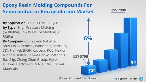
The global semiconductor market, valued at approximately $579 billion in 2022, is anticipated to reach around $790 billion by 2029, reflecting a compound annual growth rate (CAGR) of 6% over the forecast period. This growth trajectory underscores the increasing demand for semiconductors across various industries, driven by advancements in technology and the proliferation of electronic devices. The semiconductor market is a cornerstone of modern technology, providing the essential components that power everything from smartphones and computers to automobiles and industrial machinery. As industries continue to innovate and integrate more sophisticated electronic systems, the demand for semiconductors is expected to rise, fueling the market's expansion. The projected growth of the semiconductor market highlights the critical role that semiconductors play in enabling technological advancements and supporting the digital transformation of industries worldwide. This growth also emphasizes the importance of efficient and reliable semiconductor manufacturing processes, including the use of high-quality encapsulation materials like epoxy resin molding compounds, to ensure the performance and longevity of semiconductor devices. As the market continues to evolve, the need for innovative solutions and materials that can meet the demands of modern electronic applications will remain a key driver of growth in the semiconductor industry.
| Report Metric | Details |
| Report Name | Epoxy Resin Molding Compounds for Semiconductor Encapsulation Market |
| Accounted market size in year | US$ 579 billion |
| Forecasted market size in 2029 | US$ 790 billion |
| CAGR | 6% |
| Base Year | year |
| Forecasted years | 2025 - 2029 |
| by Type |
|
| by Application |
|
| Production by Region |
|
| Consumption by Region |
|
| By Company | Sumitomo Bakelite, Shin-Etsu Chemical, Panasonic, Samsung SDI, Henkel, BASF, Kyocera, KCC, Hexion, Nippon Denko, Showa Denko Materials, Raschig, Chang Chun Group, Hysol Huawei Electronics, MATFRON, Eternal Materials |
| Forecast units | USD million in value |
| Report coverage | Revenue and volume forecast, company share, competitive landscape, growth factors and trends |


