What is Global Anodic Aluminum Oxide (AAO) Wafer Market?
The Global Anodic Aluminum Oxide (AAO) Wafer Market is a specialized segment within the materials industry, focusing on the production and application of anodic aluminum oxide wafers. These wafers are created through an electrochemical process that transforms aluminum into a porous structure, offering unique properties such as high thermal stability, mechanical strength, and a highly ordered nanoporous structure. These characteristics make AAO wafers highly desirable in various technological applications, including electronics, photonics, and biotechnology. The market for these wafers is driven by the increasing demand for advanced materials that can enhance the performance and efficiency of electronic devices. As industries continue to innovate and seek materials that offer superior performance, the demand for AAO wafers is expected to grow. The market is characterized by a diverse range of applications, from serving as templates for nanostructures to being used in sensors and filtration systems. The versatility and adaptability of AAO wafers make them a critical component in the advancement of technology across multiple sectors, reflecting their growing importance in the global market landscape.
4 Inch, 6 Inch, 8 Inch, Others in the Global Anodic Aluminum Oxide (AAO) Wafer Market:
In the Global Anodic Aluminum Oxide (AAO) Wafer Market, the categorization based on size, such as 4 Inch, 6 Inch, 8 Inch, and others, plays a significant role in addressing the diverse needs of various industries. The 4-inch AAO wafers are the most prevalent, holding a substantial market share due to their widespread use in research and development as well as in small-scale production environments. These wafers are particularly favored in academic and industrial research settings where cost-effectiveness and ease of handling are crucial. Their size makes them ideal for experimental setups and prototyping, allowing researchers to explore new applications and refine existing technologies. The 6-inch AAO wafers, on the other hand, are gaining traction in industries that require a balance between size and performance. These wafers are often used in medium-scale production processes where the demand for higher throughput and efficiency is paramount. They offer a larger surface area compared to the 4-inch wafers, enabling more extensive experimentation and production capabilities. The 8-inch AAO wafers represent a significant leap in terms of production capacity and application scope. These larger wafers are primarily utilized in high-volume manufacturing environments, such as semiconductor fabrication and large-scale industrial applications. The increased surface area of the 8-inch wafers allows for the production of more complex and intricate nanostructures, catering to the needs of advanced technological applications. Additionally, the "Others" category encompasses a range of wafer sizes that cater to niche applications and specialized industries. These wafers are often customized to meet specific requirements, offering flexibility and adaptability to unique production processes. The diversity in wafer sizes within the AAO market highlights the adaptability of these materials to various industrial needs, from small-scale research to large-scale manufacturing. As the demand for advanced materials continues to rise, the market for AAO wafers of different sizes is expected to expand, driven by the need for innovative solutions across multiple sectors. The ability to tailor wafer sizes to specific applications underscores the versatility of AAO technology, making it a vital component in the advancement of modern industries.
Packaging & Foundry, IDM Enterprise in the Global Anodic Aluminum Oxide (AAO) Wafer Market:
The usage of Global Anodic Aluminum Oxide (AAO) Wafer Market in areas such as Packaging & Foundry and IDM (Integrated Device Manufacturer) Enterprise is pivotal in driving technological advancements and enhancing production efficiencies. In the Packaging & Foundry sector, AAO wafers are utilized for their exceptional properties, such as high thermal conductivity and mechanical strength, which are crucial in the packaging of electronic components. These wafers serve as substrates for the deposition of various materials, enabling the creation of intricate electronic circuits and devices. The porous structure of AAO wafers allows for efficient heat dissipation, which is essential in maintaining the performance and longevity of electronic components. This makes them an ideal choice for packaging applications where thermal management is a critical concern. In the IDM Enterprise sector, AAO wafers play a significant role in the fabrication of semiconductor devices. The unique nanoporous structure of these wafers allows for precise control over the deposition of materials, enabling the production of high-performance electronic components. IDM enterprises leverage the properties of AAO wafers to enhance the efficiency and reliability of their manufacturing processes, leading to the development of cutting-edge technologies. The versatility of AAO wafers in these sectors is further exemplified by their use in the creation of sensors and filtration systems. The ordered nanoporous structure of AAO wafers makes them ideal for applications that require high sensitivity and selectivity, such as chemical and biological sensors. In filtration systems, the porous nature of AAO wafers allows for the efficient separation of particles, making them suitable for use in various industrial and environmental applications. The integration of AAO wafers in Packaging & Foundry and IDM Enterprise sectors underscores their importance in the advancement of technology and the optimization of production processes. As industries continue to seek innovative solutions to enhance performance and efficiency, the demand for AAO wafers is expected to grow, driving further developments in these critical areas.
Global Anodic Aluminum Oxide (AAO) Wafer Market Outlook:
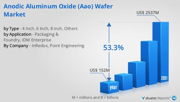
The global market for Anodic Aluminum Oxide (AAO) Wafer was valued at $152 million in 2024 and is anticipated to expand significantly, reaching an estimated size of $2,537 million by 2031, with a robust compound annual growth rate (CAGR) of 53.3% during the forecast period. North America stands out as the leading producer of AAO wafers, accounting for over 51% of the market share, highlighting its dominance in this sector. The 4-inch wafer segment emerges as the largest product category, capturing more than 34% of the market share, which underscores its widespread application and preference in various industries. In terms of application, the packaging and foundry sector is the most significant, holding a commanding share of over 77%. This dominance is indicative of the critical role that AAO wafers play in these applications, driven by their unique properties and the growing demand for advanced materials. The market outlook reflects a dynamic and rapidly evolving landscape, with significant growth opportunities across different regions and applications. As industries continue to innovate and seek materials that offer superior performance, the AAO wafer market is poised for substantial expansion, driven by technological advancements and increasing demand across various sectors.
| Report Metric | Details |
| Report Name | Anodic Aluminum Oxide (AAO) Wafer Market |
| Accounted market size in year | US$ 152 million |
| Forecasted market size in 2031 | US$ 2537 million |
| CAGR | 53.3% |
| Base Year | year |
| Forecasted years | 2025 - 2031 |
| by Type |
|
| by Application |
|
| Production by Region |
|
| Consumption by Region |
|
| By Company | InRedox, Point Engineering |
| Forecast units | USD million in value |
| Report coverage | Revenue and volume forecast, company share, competitive landscape, growth factors and trends |