What is Global Semiconductor Pellicle Market?
The Global Semiconductor Pellicle Market is a crucial segment within the semiconductor industry, focusing on the production and application of pellicles. Pellicles are thin, transparent membranes used in photolithography, a process essential for manufacturing semiconductor devices. These membranes protect photomasks from particles and contaminants during the lithography process, ensuring high precision and yield in semiconductor production. As the demand for advanced electronic devices grows, so does the need for efficient and reliable semiconductor manufacturing processes, driving the demand for pellicles. The market encompasses various types of pellicles, including those used in ArF (Argon Fluoride), KrF (Krypton Fluoride), and EUV (Extreme Ultraviolet) lithography, each catering to different technological requirements and advancements. The global semiconductor pellicle market is characterized by continuous innovation and development, as manufacturers strive to enhance the performance and durability of pellicles to meet the evolving needs of the semiconductor industry. This market is pivotal in supporting the production of increasingly complex and miniaturized semiconductor devices, which are integral to modern electronics, from smartphones to advanced computing systems. As technology advances, the role of pellicles in ensuring the efficiency and effectiveness of semiconductor manufacturing becomes ever more significant.
ArF Pellicle, KrF Pellicle, EUV Pellicle, Others in the Global Semiconductor Pellicle Market:
ArF Pellicles, KrF Pellicles, EUV Pellicles, and others represent different types of pellicles used in the semiconductor industry, each serving specific roles in the photolithography process. ArF Pellicles are designed for use with Argon Fluoride lasers, which operate at a wavelength of 193 nm. These pellicles are crucial for producing high-resolution patterns on semiconductor wafers, enabling the creation of intricate and densely packed circuits. ArF pellicles are widely used in the production of advanced semiconductor devices, such as microprocessors and memory chips, where precision and miniaturization are paramount. KrF Pellicles, on the other hand, are used with Krypton Fluoride lasers, which have a wavelength of 248 nm. While not as advanced as ArF pellicles, KrF pellicles are still essential for many semiconductor manufacturing processes, particularly in the production of less complex devices. They offer a cost-effective solution for manufacturers who do not require the extreme precision provided by ArF pellicles. EUV Pellicles are a newer development, designed for use with Extreme Ultraviolet lithography, which operates at a much shorter wavelength of 13.5 nm. EUV lithography is at the forefront of semiconductor manufacturing technology, enabling the production of even smaller and more complex devices. However, the development of EUV pellicles presents significant challenges due to the extreme conditions under which they must operate, including high energy levels and the need for exceptional transparency and durability. Despite these challenges, EUV pellicles are critical for the future of semiconductor manufacturing, as they allow for further miniaturization and increased performance of electronic devices. Other types of pellicles include those used in less common lithography processes or for specialized applications. These pellicles may be designed to withstand specific environmental conditions or to provide unique performance characteristics required for certain manufacturing processes. The development and production of these various types of pellicles require significant expertise and technological innovation, as manufacturers strive to meet the diverse needs of the semiconductor industry. Each type of pellicle plays a vital role in ensuring the efficiency and effectiveness of the photolithography process, ultimately contributing to the production of high-quality semiconductor devices that power modern technology.
IC Bumping, IC Foundry, IC Substrate, MEMS, LED Package in the Global Semiconductor Pellicle Market:
The Global Semiconductor Pellicle Market finds its application in several key areas, including IC Bumping, IC Foundry, IC Substrate, MEMS, and LED Package. In IC Bumping, pellicles are used to protect photomasks during the lithography process, ensuring the precise alignment and patterning of bumps on semiconductor wafers. These bumps are essential for creating electrical connections between the semiconductor die and the package, enabling the integration of multiple chips into a single device. The use of pellicles in IC Bumping helps to improve yield and reduce defects, resulting in more reliable and efficient semiconductor devices. In IC Foundry, pellicles play a critical role in the production of semiconductor wafers, which serve as the foundation for integrated circuits. By protecting photomasks from contaminants, pellicles help to ensure the accuracy and consistency of the lithography process, leading to higher quality and more reliable semiconductor products. This is particularly important in the foundry industry, where manufacturers produce a wide range of semiconductor devices for various applications. In the IC Substrate area, pellicles are used to protect photomasks during the production of substrates, which provide the mechanical support and electrical connections for semiconductor devices. The use of pellicles in this process helps to improve the precision and reliability of substrate manufacturing, resulting in better performance and longer lifespan for the final semiconductor products. In MEMS (Micro-Electro-Mechanical Systems), pellicles are used to protect photomasks during the fabrication of tiny mechanical and electrical components on semiconductor wafers. These components are used in a wide range of applications, from sensors and actuators to medical devices and consumer electronics. The use of pellicles in MEMS manufacturing helps to ensure the accuracy and reliability of these components, leading to better performance and increased functionality of the final products. In the LED Package area, pellicles are used to protect photomasks during the production of LED chips, which are used in a variety of lighting and display applications. By ensuring the precision and consistency of the lithography process, pellicles help to improve the efficiency and brightness of LED chips, resulting in better performance and longer lifespan for LED products. Overall, the use of pellicles in these various areas of the semiconductor industry helps to improve the quality, reliability, and performance of semiconductor devices, supporting the continued growth and advancement of modern technology.
Global Semiconductor Pellicle Market Outlook:
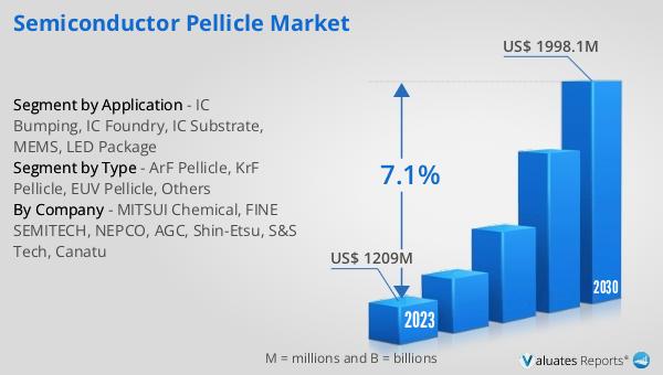
In 2024, the global market for semiconductor pellicles was valued at approximately $658 million. This market is anticipated to expand significantly, reaching an estimated size of $1,011 million by 2031. This growth represents a compound annual growth rate (CAGR) of 6.0% over the forecast period. The increasing demand for semiconductor pellicles is driven by the growing complexity and miniaturization of semiconductor devices, which require high precision and reliability in the manufacturing process. As technology continues to advance, the need for efficient and effective photolithography processes becomes more critical, further fueling the demand for pellicles. The market's growth is also supported by ongoing innovations and developments in pellicle technology, as manufacturers strive to enhance the performance and durability of these essential components. The expansion of the semiconductor pellicle market reflects the broader trends in the semiconductor industry, where the push for smaller, faster, and more powerful electronic devices drives the need for advanced manufacturing solutions. As the market evolves, it will continue to play a vital role in supporting the production of cutting-edge semiconductor devices that power modern technology.
| Report Metric | Details |
| Report Name | Semiconductor Pellicle Market |
| Accounted market size in year | US$ 658 million |
| Forecasted market size in 2031 | US$ 1011 million |
| CAGR | 6.0% |
| Base Year | year |
| Forecasted years | 2025 - 2031 |
| by Type |
|
| by Application |
|
| Production by Region |
|
| Consumption by Region |
|
| By Company | MITSUI Chemical, FINE SEMITECH, Shin-Etsu, Micro Lithography, Inc., S&S Tech, INKO, NEPCO, Canatu |
| Forecast units | USD million in value |
| Report coverage | Revenue and volume forecast, company share, competitive landscape, growth factors and trends |